Electronic device assembly structure

A technology of electronic devices and combined structures, which is applied to the construction parts of electrical equipment, circuit layout on insulating boards, circuit layout on support structures, etc., can solve problems such as difficult maintenance, occupying multiple jacks, wasting space, etc. Achieve the effect of saving time and manpower, reducing the probability of assembly errors and parts damage, and reducing manufacturing costs

Active Publication Date: 2013-10-30
GEMTEK TECH CO LTD
View PDF14 Cites 0 Cited by
  • Summary
  • Abstract
  • Description
  • Claims
  • Application Information

AI Technical Summary

Problems solved by technology

[0003] The known electronic devices each have different shapes, cannot be arranged neatly and are not easy to connect when in use, wasting a lot of unnecessary space
Moreover, different molds must be developed for the manufacture of electronic devices with different shapes, which increases the manufacturing cost and makes maintenance difficult
[0004] In addition, different electronic devices need to use multiple connecting cables to connect to the computer, which is not beautiful and occupies multiple jacks

Method used


Image

  • Electronic device assembly structure
  • Electronic device assembly structure
  • Electronic device assembly structure

Examples


Embodiment 1

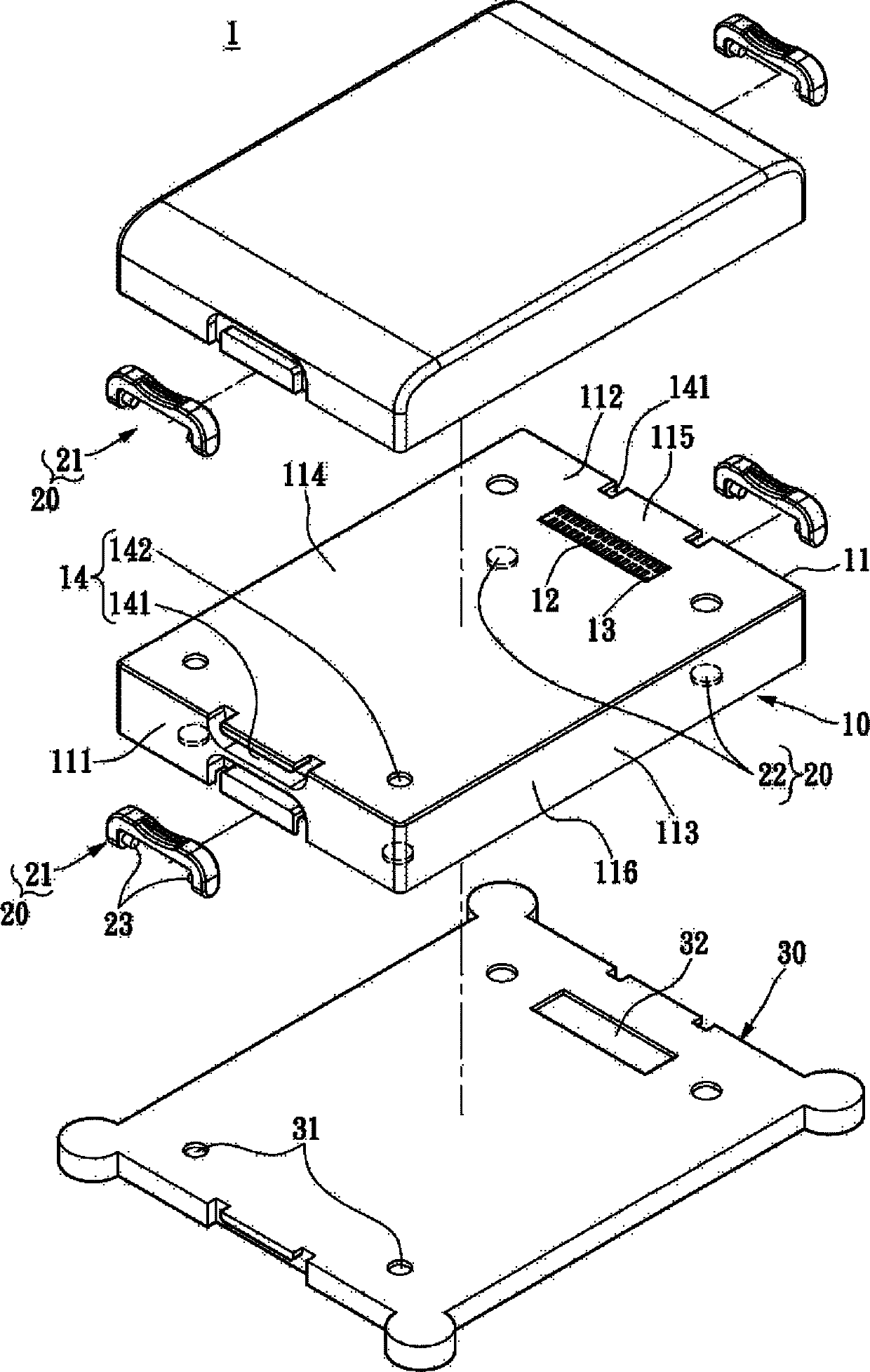
[0060] see Figure 1A , Figure 1A It is a three-dimensional exploded view of the electronic device assembly structure of the present invention, which shows the electronic device assembly structure 1 of the present invention, and the electronic device assembly structure 1 includes at least two electronic devices 10 and a fixed connection unit 20 . The number of electronic devices 10 below is described as two, but not limited thereto.

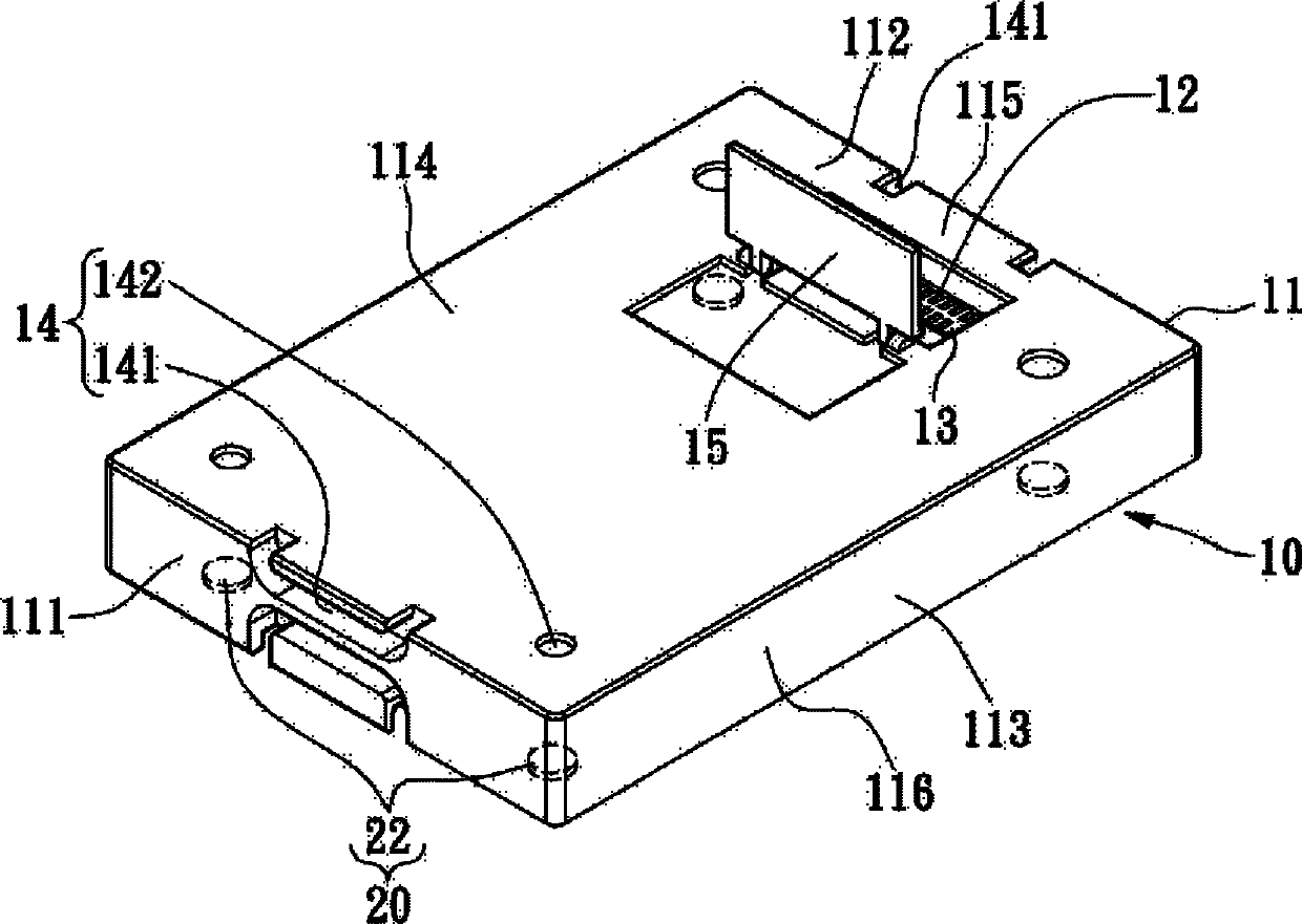
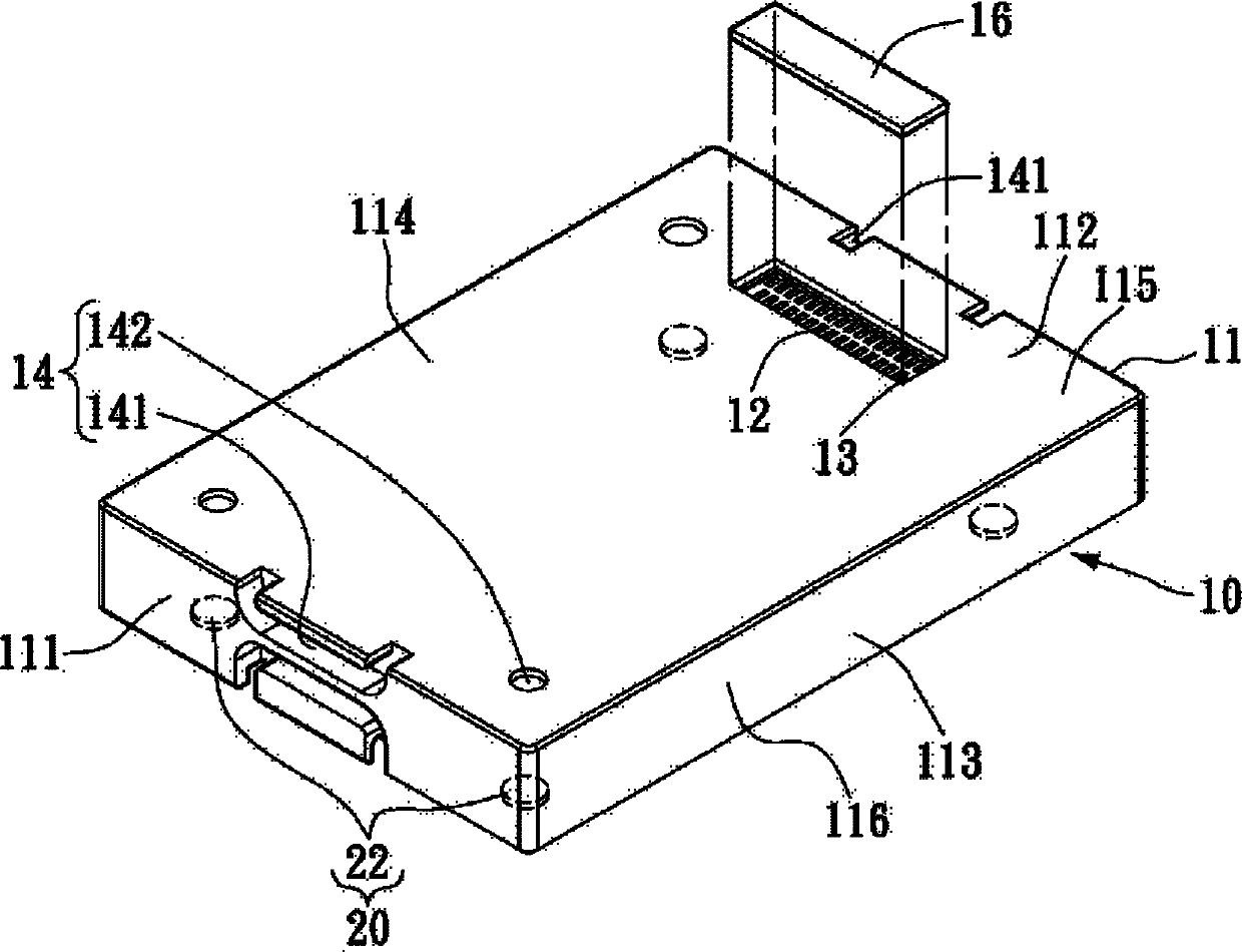
[0061] In this embodiment, one of the electronic devices 10 is stacked on the other electronic device 10, each electronic device 10 includes a body 11 and an electrical connection module 12, and at least one opening 13 is formed on the body 11 , the electrical connection module 12 is arranged in the body 11, the fixed connection unit 20 is connected to two electronic devices 10, and is used to assemble the two electronic devices 10 into one body, and the electrical connection module 12 of one of the electronic devices 10 The electrical connectio...

Embodiment 2

[0075] see Figure 4 , Figure 5A and Figure 5B , which shows the second embodiment of the combined structure 1' of the electronic device of the present invention. The fixed connection unit 20' includes a plurality of connection arms 21'.

[0076] Specifically, the plurality of connection grooves 141' are recessed at the periphery of the upper side wall 111 of the body 11, and the plurality of connection arms 21' are formed by extending from the periphery of the lower side wall 112 of the body 11 and correspond to the A plurality of connecting grooves 141', more specifically, the connecting groove 141' is composed of a side groove wall 1411' and a bottom groove wall 1412', wherein the side groove wall 1411' is also provided with an elastic first The engaging structure 1413', the outer wall of the connecting arm 21' is provided with a non-elastic second engaging structure 22', the first engaging structure 1413' and the second engaging structure 22' can be semi-cylindrical ...


PUM


Abstract

An electronic device assembly structure comprises two electronic devices and a fastening unit. Each electronic device includes a body and an electric connection module. The body has at least one opening formed thereon. The electric connection module is located in the body. The fastening unit fastens the two electronic devices together in an integrated manner. The electric connection modules of the two electronic devices form electric connection through the opening.

Description

technical field [0001] The invention relates to an electronic device combination, in particular to an electronic device combination structure with a modularized electronic device and a connection module. Background technique [0002] Modern people's lives are surrounded by many electronic products, especially computers. More and more electronic devices are beginning to be connected with computers, which can use computers as power sources or to transmit data. [0003] The known electronic devices each have different shapes, cannot be arranged neatly and are not easy to connect when in use, and a lot of unnecessary space is wasted. Moreover, different molds must be developed for the manufacture of electronic devices with different shapes, which increases the manufacturing cost and makes maintenance difficult. [0004] In addition, connecting different electronic devices to the computer requires multiple connection cables, which is not beautiful and occupies multiple jacks. ...

Claims


Application Information

Patent Timeline
Patent Type & Authority Applications(China)
IPC IPC(8): H05K7/00G06F1/16H01R12/51H01R12/52
CPCH05K7/06H05K7/005H05K5/0021H05K7/023
Inventor 林荣兴朱其全颜志旭
Owner GEMTEK TECH CO LTD
Why Eureka
Try Eureka