bosch etching method

A technology of etching holes and etching gas, which is applied in the fields of electrical components, semiconductor/solid-state device manufacturing, circuits, etc., can solve the problems that the stability of the etching process needs to be improved, and achieve fast etching directionality and high etching morphology. Good, less loss effect

Active Publication Date: 2015-09-30
ADVANCED MICRO FAB EQUIP INC CHINA
View PDF5 Cites 0 Cited by
  • Summary
  • Abstract
  • Description
  • Claims
  • Application Information

AI Technical Summary

Problems solved by technology

[0005] However, in the prior art Bosch (Bosch) etching process, the stability of the etching process still needs to be improved

Method used


Image

  • bosch etching method
  • bosch etching method
  • bosch etching method

Examples


Embodiment B

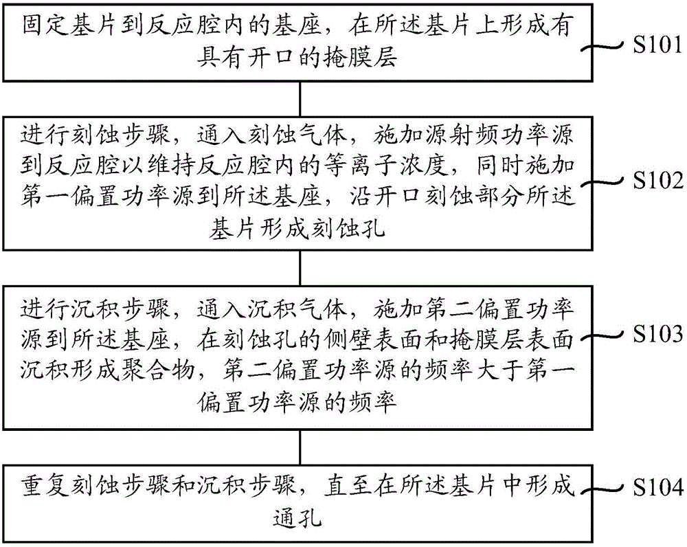
[0028] figure 1 It is a schematic flow diagram of the Bosch etching method of the embodiment of the present invention, including:

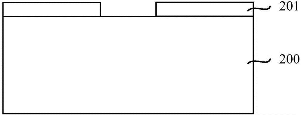
[0029] Step S101, fixing the substrate to the base in the reaction chamber, and forming a mask layer with openings on the substrate;

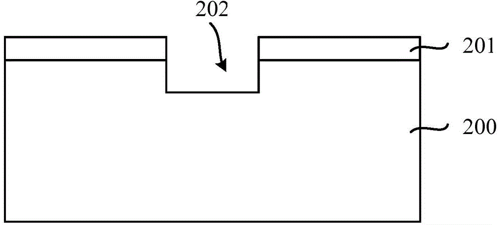
[0030] Step S102, performing an etching step, feeding an etching gas, applying a source radio frequency power source to the reaction chamber to maintain the plasma concentration in the reaction chamber, and simultaneously applying a first bias power source to the base, and etching a part along the opening The substrate forms etching holes;

[0031]Step S103, performing a deposition step, passing a deposition gas, applying a second bias power source to the base, depositing and forming a polymer on the sidewall surface of the etched hole and the surface of the mask layer, and the second bias power source a frequency greater than that of the first bias power source;

[0032] Step S104, repeating the etching step an...


PUM


Abstract

The invention provides a Bosch etching method. The method comprises the following steps: a substrate is fixed on a base in a reaction chamber, and a mask layer with an opening is formed on the substrate; etching is performed: etching gas is piped in, a source radio frequency power source is applied to the reaction chamber so as to maintain plasma concentration in the reaction chamber, meanwhile, a first bias power source is applied to the base, and partial substrate is etched along the opening so as to form an etching hole; deposition is performed: deposition gas is piped in, a second bias power source is applied to the base, deposition is performed on the side wall surface of the etching hole and the surface of the mask layer so as to form a polymer, wherein the frequency of the second bias power source is larger than that of the first bias power source; etching and deposition are performed repeatedly until a through hole is formed in the substrate. The Bosch etching method provided by the invention can guarantee the etching rate, and meanwhile has higher stability.

Description

technical field [0001] The invention relates to the field of semiconductor manufacturing, in particular to a Bosch etching method. Background technique [0002] With the continuous development of semiconductor technology, the feature size of semiconductor devices has become very small. It is becoming more and more difficult to increase the number of semiconductor devices in a two-dimensional packaging structure. Therefore, three-dimensional packaging has become a method that can effectively improve chip integration. degree method. Current three-dimensional packaging includes gold wire bonding-based chip stacking (Die Stacking), package stacking (Package Stacking) and three-dimensional (3D) stacking based on Through Silicon Via (TSV). Among them, the three-dimensional stacking technology using through-silicon vias has the following three advantages: (1) high-density integration; (2) greatly shortening the length of electrical interconnections, which can well solve the proble...

Claims


Application Information

Patent Timeline
Patent Type & Authority Patents(China)
IPC IPC(8): H01L21/768
Inventor 梁洁李俊良
Owner ADVANCED MICRO FAB EQUIP INC CHINA
Why Eureka
Try Eureka