Mask plate and manufacturing method thereof

A manufacturing method and mask plate technology, applied in the field of semiconductors, can solve problems such as photoresist patterns with inconsistent heights on the upper surface

Inactive Publication Date: 2013-11-27
NANTONG FUJITSU MICROELECTRONICS
View PDF4 Cites 12 Cited by
  • Summary
  • Abstract
  • Description
  • Claims
  • Application Information

AI Technical Summary

Problems solved by technology

[0007] The problem to be solved by the present invention is: it is impossible to form a photoresist pattern with inconsistent ...

Method used


Image

  • Mask plate and manufacturing method thereof
  • Mask plate and manufacturing method thereof
  • Mask plate and manufacturing method thereof

Examples


no. 1 example

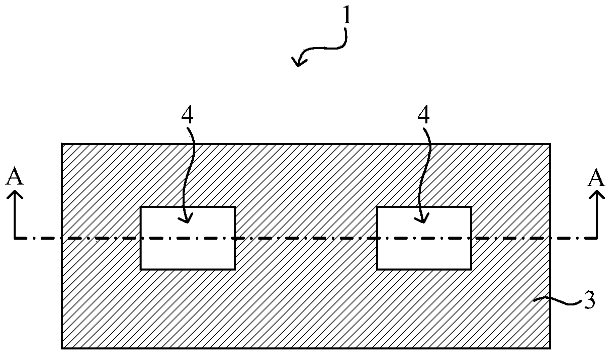
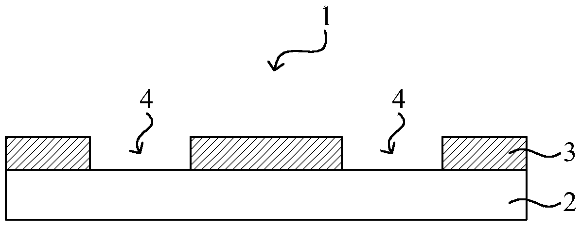
[0046] combine Figure 4 and Figure 5 As shown, the mask plate 100 includes: a transparent substrate 110 ; a patterned light-shielding layer 120 on the transparent substrate 110 , and the patterned light-shielding layer 120 has an opening 130 exposing the transparent substrate 110 . The regions corresponding to the openings 130 on the mask 100 are all light-transmitting regions.

[0047] The opening 130 is divided into a first opening unit 131 and a second opening unit 132 , the bottom of the first opening unit 131 exposes the transparent substrate 110 , and the bottom of the second opening unit 132 is covered with a transparent film 140 . Therefore, the light-transmitting area of ​​the mask plate 100 is divided into a first light-transmitting area and a second light-transmitting area, wherein, the area corresponding to the first opening unit 131 on the mask plate 100 is the first light-transmitting area, and The area corresponding to the second opening unit 132 is the seco...

no. 2 example

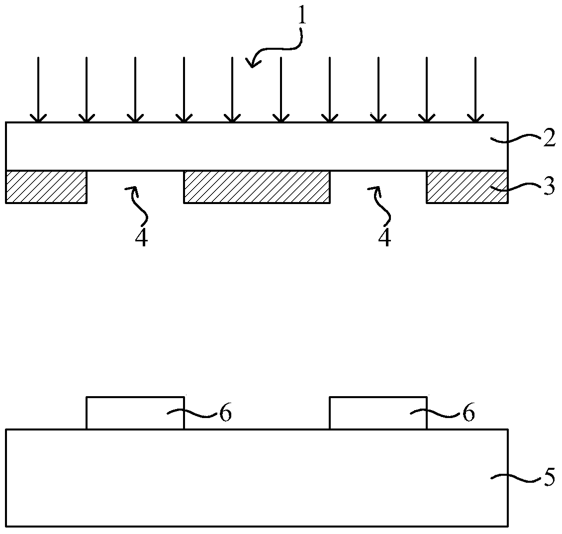
[0071] The difference between the second embodiment and the first embodiment is that in the second embodiment, the combination Figure 10 and Figure 11 As shown, the transparent substrate 110 below the second opening unit 132 in the opening 130 is doped with a metal 180 . After the transparent substrate 110 is doped with metal 180, the light transmittance of the transparent substrate will decrease. Therefore, the light transmittance of the area corresponding to the first opening unit 131 on the mask plate (that is, the first light-transmitting area) is greater than that of the mask plate. The light transmittance of the area on the stencil corresponding to the second opening unit 132 (ie, the second light transmission area).

[0072] In this embodiment, the entire thickness of the transparent substrate 110 under the second opening unit 132 is doped with metal 180 .

[0073] In this embodiment, the metal 180 is chromium. In other embodiments, the metal 180 may also be other ...


PUM

PropertyMeasurementUnit
Thicknessaaaaaaaaaa

Abstract

The invention relates to a mask plate and a manufacturing method thereof. The mask plate comprises a transparent base plate and a graphical shading layer, wherein the graphical shading layer is positioned on the transparent base plate; the graphical shading layer is provided with an opening from which the transparent base plate can be exposed out; the opening is at least divided into a first opening unit and a second opening unit; the area on a mask plate body and corresponding to the first opening unit serves as a first light-transmitting area, and the area on the mask plate body and corresponding to the second opening unit serves as a second light-transmitting area; the bottom of the first opening unit is exposed out of the transparent base plate; the light transmittance of the second light-transmitting area is less than that of the transparent base plate. Light resistance patterns with different-height upper surfaces can be formed at the positions on a light resistance layer and corresponding to the light-transmitting areas of the mask plate by utilizing the mask plate.

Description

technical field [0001] The invention relates to the technical field of semiconductors, in particular to a mask plate and a manufacturing method thereof. Background technique [0002] The mask plate is widely used in the semiconductor manufacturing process, and is mainly used for patterned shielding of the device to be exposed coated with photoresist on the surface during exposure, so as to realize the selective exposure of the device to be exposed. [0003] like figure 1 and figure 2 As shown, the existing mask plate 1 includes: a transparent substrate 2 ; a patterned light-shielding layer 3 located on the transparent substrate 2 , and the patterned light-shielding layer 3 has an opening 4 exposing the transparent substrate 2 . The area corresponding to the opening 4 on the mask plate 1 is a light-transmitting area. [0004] like image 3 As shown, the photoresist layer (not shown) on the device 5 to be exposed is exposed by using the mask plate 1, and then the photores...

Claims


Application Information

Patent Timeline
IPC IPC(8): G03F1/54G03F1/62G03F1/80
Inventor 朱桂林高国华
Owner NANTONG FUJITSU MICROELECTRONICS
Why Eureka
Try Eureka