Multi-input boost converter based on Switch-Capacitor networks
A boost converter, multi-input technology, applied in the direction of conversion equipment without intermediate conversion to AC, can solve the problems of insufficient boost capacity and low component utilization, and achieve strong boost capacity and component utilization High, small capacitive voltage stress effect
- Summary
- Abstract
- Description
- Claims
- Application Information
AI Technical Summary
Problems solved by technology
Method used
Image
Examples
Embodiment 1
[0024] Embodiment 1, multi-input boost converter based on Switch-Capacitor network
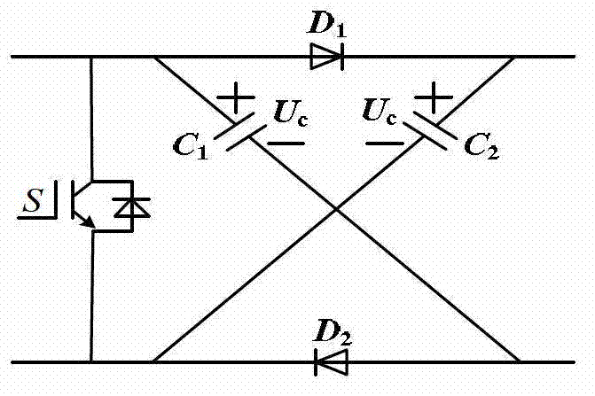
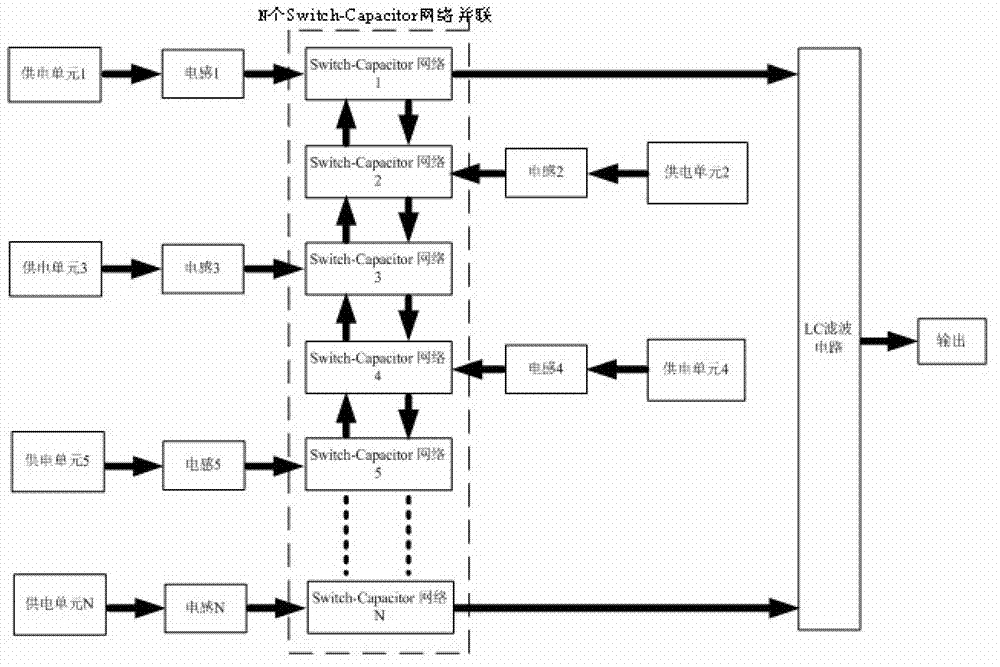
[0025] The circuit structure of the new energy combined power supply system based on the multi-input boost converter based on the Switch-Capacitor network is as follows: figure 2 shown. Any input voltage is boosted through the parallel accumulation of multiple Switch-Capacitor networks, and then through the LC filter circuit to achieve an output voltage with smaller ripples. The input source is connected to any Switch-Capacitor network, and its input voltage will achieve the same output voltage through the accumulation of all network capacitor voltages, that is, each network contributes a part of the voltage to the output terminal, which is the multi-input boost converter. uniqueness. Therefore, compared with the existing multi-input converter, the multi-input boost converter greatly improves the utilization rate of components.
[0026] Depending on the number of Switch-Capacitor networks ...
Embodiment 2
[0037] Embodiment 2, taking power supply unit 1 as an example (power supply unit 1 chooses any one of photovoltaic power supply unit, fuel cell power supply unit and wind energy power supply unit)
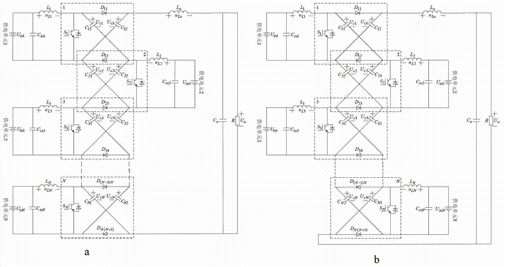
[0038] In the new energy joint power supply system, when only the power supply unit 1 supplies power, the circuit topology of the three-input boost converter is as follows Figure 5 As shown, the equivalent circuit is as Figure 6 as shown, Figure 6 (a) is the switch on, (b) is the switch off. The three-input boost converter obtains a higher output voltage through accumulative boosting of capacitor voltages in three Switch-Capacitor networks.
[0039] When the three switches S 1 , S 2 , S 3 While conducting, the diode D 11 、D 12 、D 23 、D 34 are turned off, the equivalent circuit such as Figure 6 (a) shown. At this point, the capacitor C in network 1 11 with C 12 , the capacitor C in network 2 21 with C 22 and capacitor C in network 3 31 with C 32 respectively int...
Embodiment 3
[0047] Embodiment 3, taking the power supply unit 2 as an example (the power supply unit 2 chooses any one of photovoltaic power supply unit, fuel cell power supply unit and wind energy power supply unit)
[0048] When only the power supply unit 2 supplies power, the circuit topology of the three-input boost converter is as follows Figure 7 As shown, the equivalent circuit is as Figure 8 as shown, Figure 8 (a) is the switch on, (b) is the switch off. In this case, the working principle of the three-input boost converter is the same as when only the power supply unit 1 supplies power, and the voltages of the capacitors in the three Switch-Capacitor networks are accumulated and boosted to obtain a higher output voltage.
[0049] When the three switches S 1 , S 2 , S 3 When turned on simultaneously, the equivalent circuit such as Figure 8 (a) shown. At this time, the inductance L 2 and inductance L o The magnitudes of the voltages on are:
[0050] u L2 =U in2 ...
PUM
 Abstract
Description
Claims
Application Information


