Image pickup unit and image pickup display system

A technology of an imaging device and a photoelectric conversion device, which is applied in the field of X-ray imaging technology, can solve problems such as leakage current, shot noise, and image quality degradation, so as to reduce the influence of shot noise, improve imaging quality, and suppress current leakage Effect

Inactive Publication Date: 2013-12-18
SONY SEMICON SOLUTIONS CORP
View PDF6 Cites 1 Cited by
  • Summary
  • Abstract
  • Description
  • Claims
  • Application Information

AI Technical Summary

Problems solved by technology

[0005] However, with the double-gate structure transistor disclosed in Japanese Unexamined Application Publication No. 2004-265935, leakage current may occur when switching from an on operation to an off operation, as compared with a general-type single-gate structure transistor. Leads to the so-called shot noise (shot noise)
There is thus a disadvantage that image quality is degraded due to this noise

Method used


Image

  • Image pickup unit and image pickup display system
  • Image pickup unit and image pickup display system
  • Image pickup unit and image pickup display system

Examples


Embodiment

[0044] structure

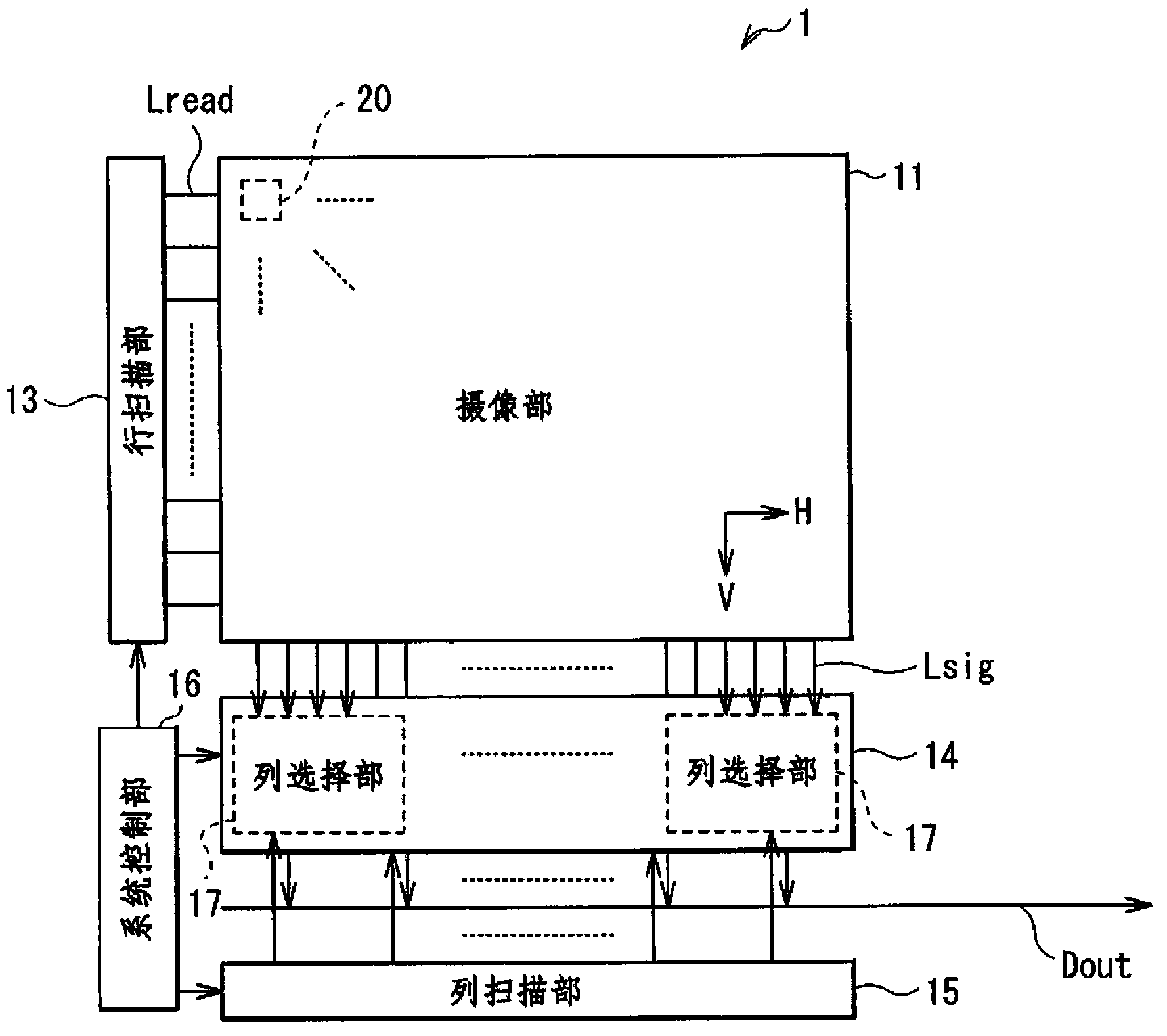
[0045] figure 1 The overall block configuration of the imaging device (imaging device 1 ) of the embodiment of the present invention is shown. The imaging device 1 reads information of an object (acquires an image of the object) based on incident light (imaging light). The imaging device 1 includes an imaging unit 11 , a row scanning unit 13 , an A / D converting unit 14 , a column scanning unit 15 , and a system control unit 16 .

[0046] camera department 11

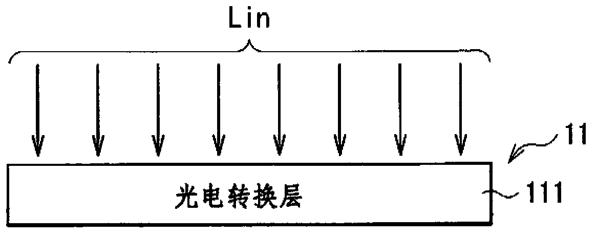
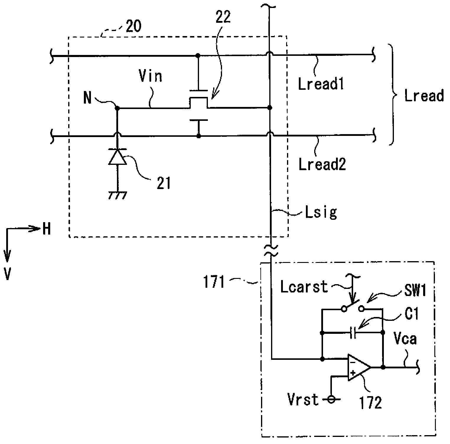
[0047] The imaging unit 11 generates an electrical signal depending on incident light (imaging light). In the imaging section 11, pixels (imaging pixels, unit pixels) 20 can be two-dimensionally arranged in a row-column pattern (matrix pattern), and each pixel 20 has a photoelectric conversion device (photoelectric conversion device 21 described below), a photoelectric The conversion means generates photoelectric charges having a charge amount corresponding to the amount of imaging light, and inter...

example 1-1

[0080] Image 6 A cross-sectional structure of a transistor (transistor 22A) of Modification Example 1-1 is shown. Like the transistor 22 in the above-mentioned embodiment of the present invention, a transistor 22A and a photoelectric conversion device 21 are provided in each pixel 20 of the imaging unit 11 of the above-mentioned imaging device 1 . In the transistor 22A of this modified example, the gate electrodes 120A and 120B are arranged to face each other with the semiconductor layer 126 arranged therebetween, and the LDD layers 126b1 and 126b2 may be formed adjacent to the source side and the channel layer 126a in the semiconductor layer 126 . Both ends 126e1 and 126e2 on the drain side. In this configuration, like the configurations of the above-described embodiments of the present invention, the transistor 22A also has a non-overlapping region d2 corresponding to the drain-side end 126e2 of the channel layer 126a.

[0081] However, the transistor 22A of the present m...

example 1-2

[0085] Figure 8 A cross-sectional structure of the transistor (transistor 22B) of Modification Example 1-2 is shown. Like the transistor 22 in the above-described embodiment of the present invention, a transistor 22B and a photoelectric conversion device 21 are provided in each pixel 20 of the imaging unit 11 of the imaging device 1 described above. In the transistor 22B of the present modified example, the gate electrodes 120A and 120B are arranged to face each other with the semiconductor layer 126 arranged therebetween. Like the above-described embodiments of the present invention, the transistor 22B has a non-overlapping region d2 corresponding to the drain-side end 126e2 of the channel layer 126a.

[0086] However, in the transistor 22B of the present modification example, in the semiconductor layer 126 , the LDD layer 126 b 2 is formed adjacent to only the end portion 126 e 2 on the drain side of the channel layer 126 a. Figure 9 An example of the planar layout confi...


PUM


Abstract

The present invention relates to an image pickup unit and an image pickup display system with the same. The image pickup unit comprises a plurality of pixels. Each pixel comprises the following components: a photoelectric conversion unit which is configured to convert incident electromagnetic radiation into an electric signal; and at least one transistor which comprises a first gate electrode and a second gate electrode above the first gate electrode. The first gate electrode and the second gate electrode do not overlap each other within a non-overlapping region. According to the image pickup unit, shot noise can be restrained thereby improving image pickup quality.

Description

technical field [0001] The invention relates to an imaging device and a display system using the imaging device. The imaging device is suitable for X-ray imaging technology widely used in medical treatment and non-injury detection. Background technique [0002] In recent years, imaging devices such as human chest X-ray imaging devices that obtain radiation-based images as electrical signals without using radiographic films have been developed. In this type of imaging device, a field-effect thin film transistor (TFT) for reading accumulated signal charges is arranged on each pixel, and an electric signal based on a radiation amount is obtained by using a pixel circuit including the transistor. [0003] Usually, a transistor employing a single gate structure, such as a so-called top-gate transistor or a bottom-gate transistor, is used as such a transistor. However, with the aforementioned imaging device for obtaining images based on radiation, it is known that, especially whe...

Claims


Application Information

Patent Timeline
Patent Type & Authority Applications(China)
IPC IPC(8): H01L27/146H04N5/335H04N5/341
CPCH01L27/14658H01L27/146H01L27/14614
Inventor 山田泰弘高德真人
Owner SONY SEMICON SOLUTIONS CORP
Why Eureka
Try Eureka