LED chip and manufacturing method thereof

A technology for light-emitting diodes and a manufacturing method, which is applied to semiconductor devices, electrical components, circuits, etc., can solve the problems of reducing the service life of light-emitting diodes, uneven brightness of light output, heat accumulation at electrodes, etc., so as to improve the uniformity of current diffusion. , The brightness is uniform, the effect of improving the service life

Active Publication Date: 2014-01-29
ZHANJING TECH SHENZHEN +1
View PDF3 Cites 1 Cited by
  • Summary
  • Abstract
  • Description
  • Claims
  • Application Information

AI Technical Summary

Problems solved by technology

However, the current of the light-emitting diode grains is easy to concentrate around the P electrode and the N electrode during the light-emitting process, so that the light-emitting brightness of the light-emitting diode grains is the largest near the two electrodes, resulting in uneven light-emitting brightness; and, the concentration of the current It is easy to cause heat accumulation at the electrode, resulting in a high temperature there and reducing the service life of the LED grain

Method used


Image

  • LED chip and manufacturing method thereof
  • LED chip and manufacturing method thereof
  • LED chip and manufacturing method thereof

Examples


Embodiment Construction

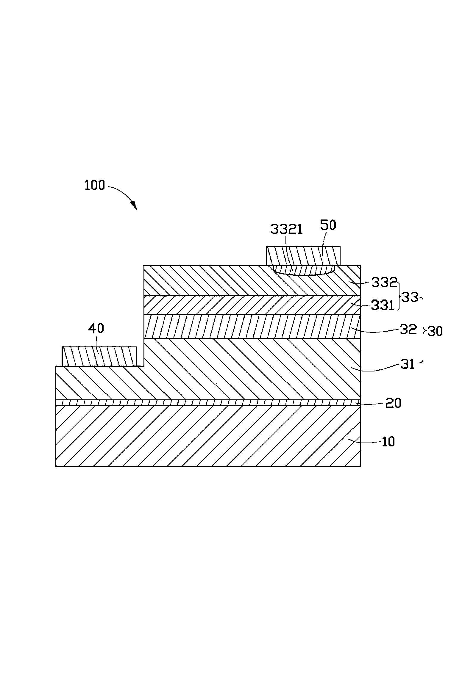
[0018] Such as figure 1 The light emitting diode die 100 provided by the first embodiment of the present invention includes in turn: a substrate 10, a buffer layer 20 formed on the substrate 10, and an epitaxial layer 30 formed on the buffer layer 20.

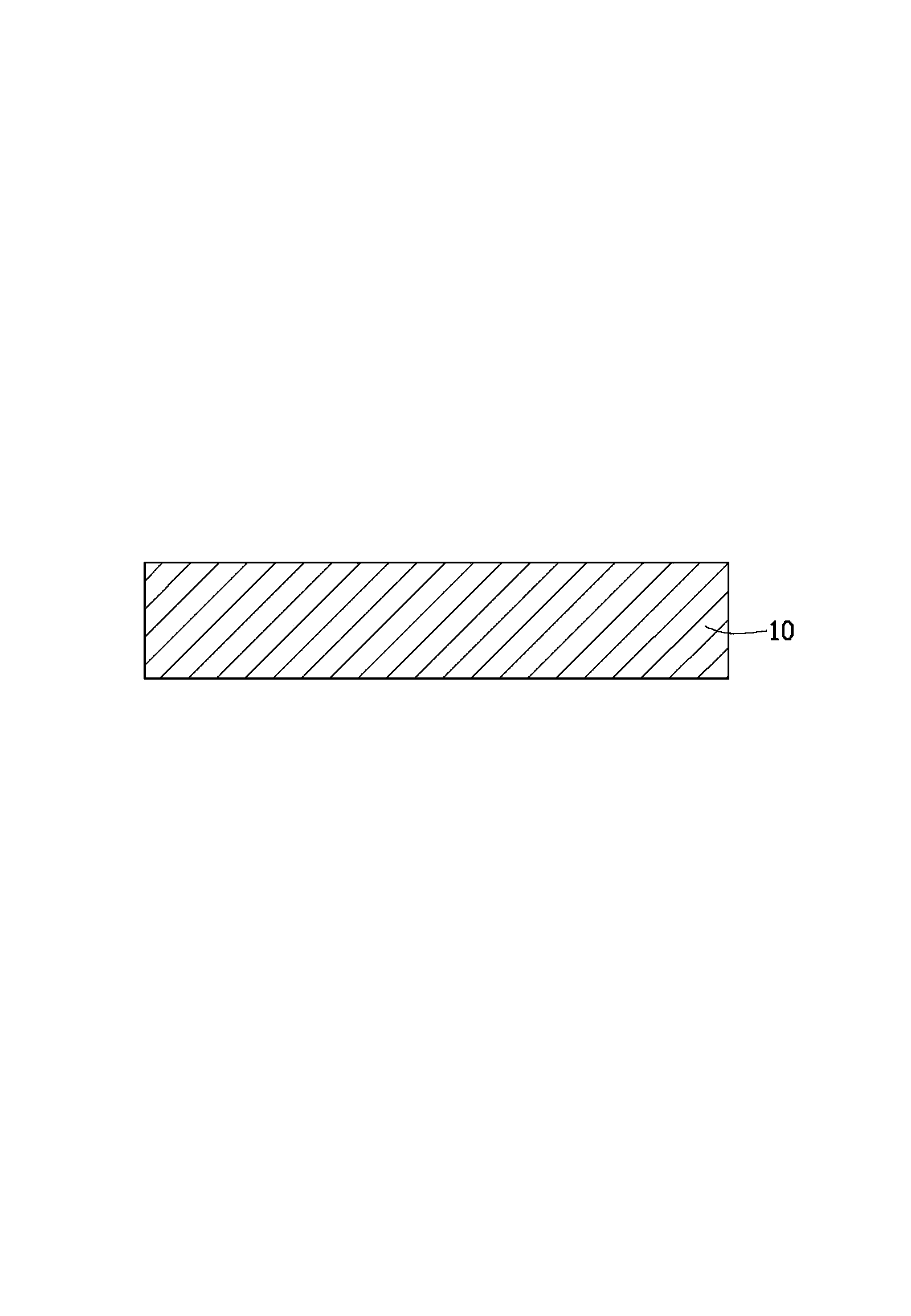
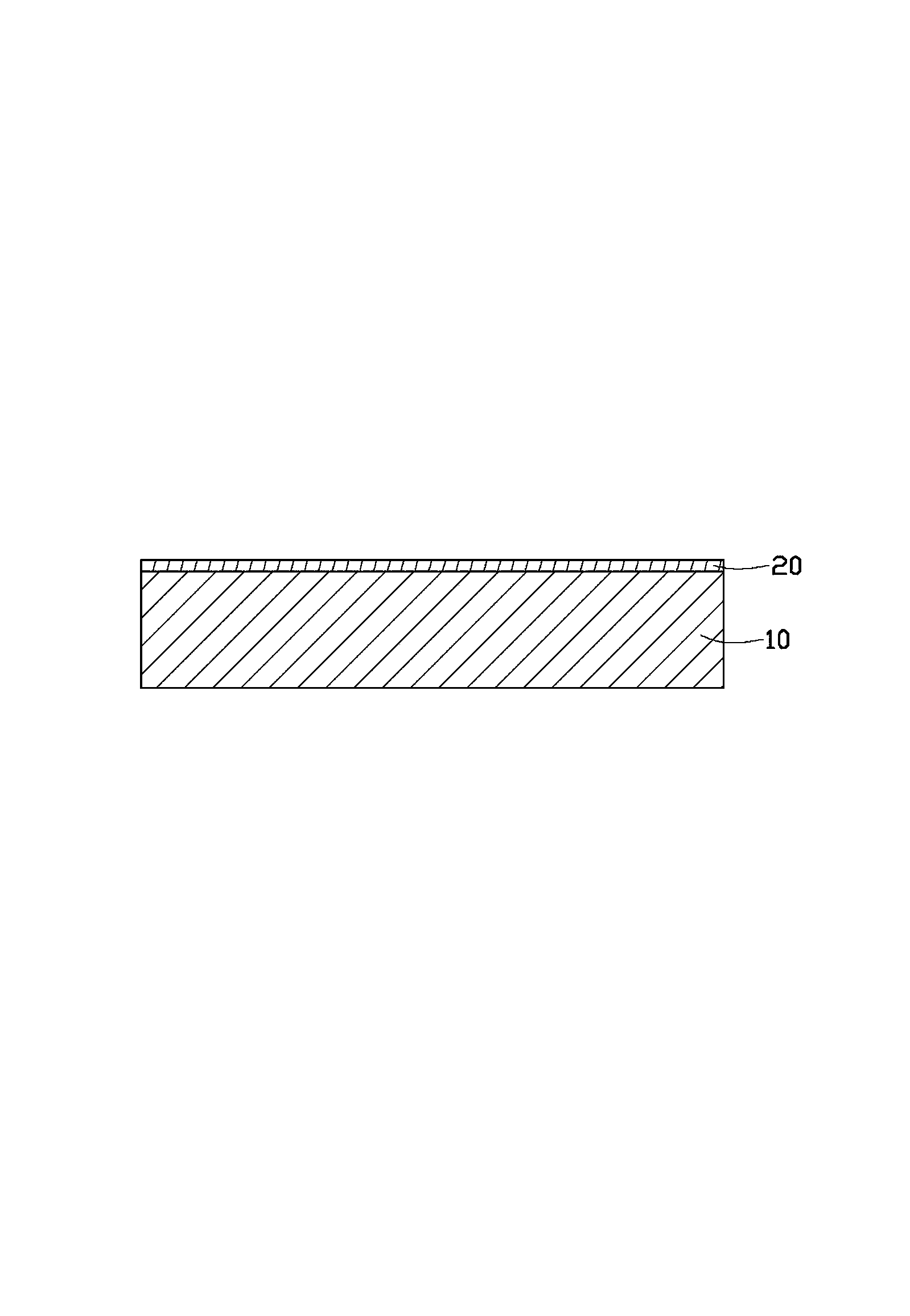
[0019] The substrate 10 can be made of sapphire, silicon carbide (SiC), silicon (Si), gallium nitride (GaN) and other materials. In this embodiment, it is preferably sapphire to control the manufacturing cost of the light-emitting chip.

[0020] The buffer layer 20 can be achieved by metal-organic chemical vapor deposition (MOCVD), molecular beam epitaxy (MBE) or hydride vapor phase epitaxy (HVPE), etc. The method grows on the surface of the substrate 10. Since the buffer layer 20 is formed to reduce defects caused by the lattice mismatch during the growth of the epitaxial layer 30, it can be made of a material whose lattice constant matches the epitaxial layer 30.

[0021] The epitaxial layer 30 can also be deposited by metal-organi...


PUM


Abstract

A light emitting diode (LED) includes a substrate and an eputaxial layer on the substrate. The epitaxial layer includes a N-type GaN-based layer, a light emitting layer, and a P-type GaN-based layer. The LED further includes a first electrode on the N-type GaN-based layer and a second electrode on the P-type GaN-based layer. The P-type GaN-based layer has a inactive portion, and the second electrode is located and covers the inactive portion.

Description

Technical field [0001] The invention relates to a light-emitting diode crystal particle and a manufacturing method thereof, in particular to a light-emitting diode crystal particle with uniform light output and a manufacturing method thereof. Background technique [0002] A light emitting diode (Light Emitting Diode, LED) is a semiconductor element that can convert current into light in a specific wavelength range. Light-emitting diodes have the advantages of high brightness, low working voltage, low power consumption, easy matching with integrated circuits, simple driving, and long life, so they can be widely used as light sources in the lighting field. [0003] The existing light emitting diode die usually includes a substrate, a semiconductor light emitting structure grown on the surface of the substrate, and a P electrode and an N electrode formed on the semiconductor light emitting structure. However, during the light-emitting process of the light-emitting diode die, the curr...

Claims


Application Information

Patent Timeline
Patent Type & Authority Applications(China)
IPC IPC(8): H01L33/14H01L33/00
CPCH01L33/32H01L33/0075H01L33/007H01L33/145
Inventor 林雅雯黄世晟凃博闵
Owner ZHANJING TECH SHENZHEN
Why Eureka
Try Eureka