How to make a circuit board

A manufacturing method and circuit board technology, which is applied in the direction of assembling printed circuits with electrical components, can solve problems such as hard punching, failure of circuit boards, and cracking of electronic components

Inactive Publication Date: 2016-05-04
AVARY HLDG (SHENZHEN) CO LTD +1
View PDF3 Cites 0 Cited by
  • Summary
  • Abstract
  • Description
  • Claims
  • Application Information

AI Technical Summary

Problems solved by technology

However, when the appearance of the electronic components is close to the appearance of the circuit board, it will cause the problem that it is difficult to punch after assembly, and it may also make the electronic components crack when punching, resulting in the failure of the circuit board

Method used


Image

  • How to make a circuit board
  • How to make a circuit board
  • How to make a circuit board

Examples


Embodiment Construction

[0074] The manufacturing method of the circuit board provided by the technical solution will be further described in detail below with reference to the drawings and multiple embodiments.

[0075] The method for manufacturing a circuit board provided in the first embodiment of the technical solution includes steps:

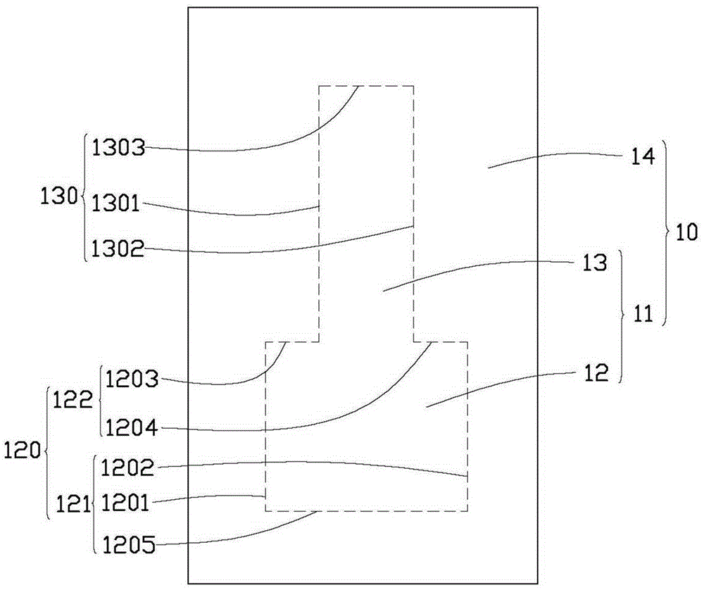
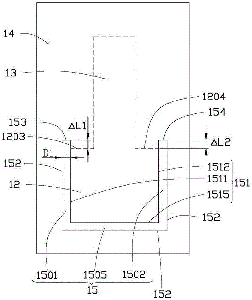
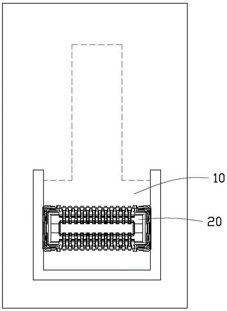
[0076] For a first step, see figure 1 , providing a circuit substrate 10 , the circuit substrate 10 includes a circuit board unit 11 and a waste portion 14 surrounding and connecting the circuit board unit 11 . The circuit board unit 11 is a finished circuit board unit to be assembled with electronic components and to be separated from the waste part 14 by punching after completing the steps of drilling, electroplating, circuit making, solder mask printing and the like. Those skilled in the art can understand that the surface of the circuit board unit 11 has a solder resist layer and connection pads exposed from the solder resist layer, etc. figure 1 The circuit ...


PUM


Abstract

The invention provides a circuit board manufacturing method which includes the steps: providing a circuit substrate comprising a circuit board unit and a waste portion; punching along a first junction portion for the first time to separate part of a first product area from the waste portion; assembling electronic components on the part of the first product area; punching along a second junction portion and the junction line of a second product area and the waste portion for the second time to separate the circuit board unit from the waste portion. The circuit board unit comprises the first product area and the second product area, the junction line of the first product area and the waste portion comprises the first junction portion and the second junction portion, the first junction portion comprises a first product side and a second product side, the second junction portion comprises a third product side and a fourth product side, the included angle between the first product side and the third product side intersected in the first product area ranges from 0 degree to 180 degrees, the included angle between the second product side and the fourth product side intersected in the first product area ranges from 0 degree to 180 degrees, and the distance between each electronic component and the first junction portion is shorter than 5mm.

Description

technical field [0001] The invention relates to circuit board technology, in particular to a method for manufacturing a circuit board assembled with electronic components. Background technique [0002] In the information, communication and consumer electronics industries, circuit boards are an indispensable and basic component of all electronic products. With the development of electronic products in the direction of miniaturization and high speed, circuit boards are also developing from single-sided circuit boards to double-sided circuit boards and multi-layer circuit boards, and more and more electronic components are assembled on circuit boards. [0003] Generally speaking, electronic components are assembled on the circuit board before punching. On the one hand, waste materials are used to partially support and align to ensure the accuracy of assembly. On the other hand, it is also convenient for batch assembly, which is conducive to improving assembly efficiency. Howev...

Claims


Application Information

Patent Timeline
Patent Type & Authority Patents(China)
IPC IPC(8): H05K3/30
Inventor 郑晓峰
Owner AVARY HLDG (SHENZHEN) CO LTD
Why Eureka
Try Eureka