Inspection device
An inspection device and image technology, applied in photovoltaic power generation, optical testing flaws/defects, etc., to achieve the effect of high-precision defect detection
- Summary
- Abstract
- Description
- Claims
- Application Information
AI Technical Summary
Problems solved by technology
Method used
Image
Examples
no. 1 Embodiment approach
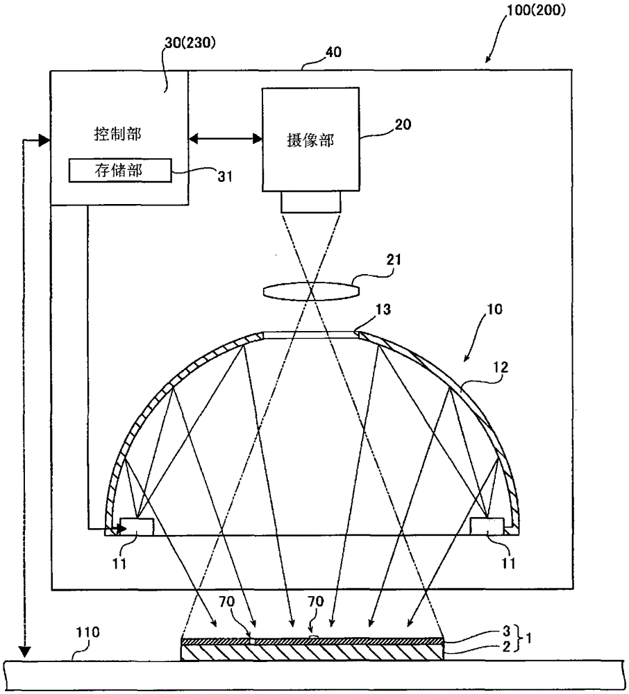
[0067] First, refer to figure 1 The overall configuration of the visual inspection device 100 according to the first embodiment of the present invention will be described. In the first embodiment, an example in which the present invention is applied to an appearance inspection device 100 for inspecting defects of an antireflection film formed on the surface of a solar cell (surface defect of a solar cell) will be described.
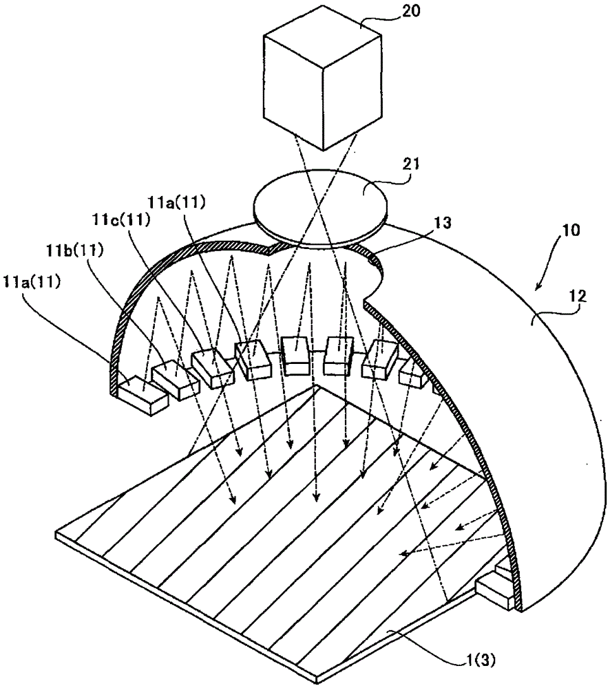
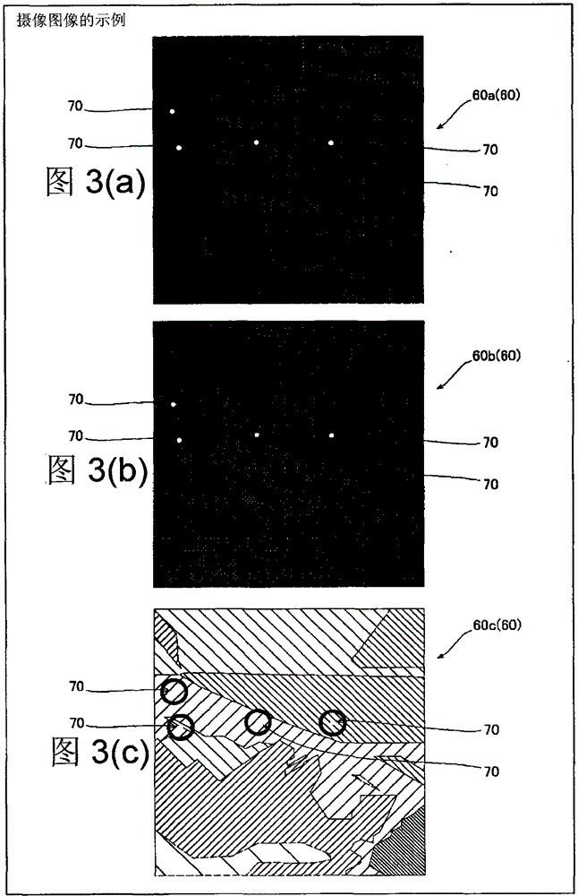
[0068] The appearance inspection device 100 of the first embodiment is an inspection device that is installed on a production line in the production process of the solar cell 1 and performs an inline inspection. The solar cell 1 includes: a semiconductor substrate 2 (hereinafter referred to as substrate 2 ); and an antireflection film 3 formed on a surface (light-receiving surface) of the substrate 2 . in addition, figure 1 In the figure, for the sake of convenience, the thickness of the solar cell 1 is enlarged to schematically show each layer (the sub...
no. 2 Embodiment approach
[0110] Second, refer to figure 1 , Figure 6(a), Figure 6(b) to Figure 9 The appearance inspection device 200 according to the second embodiment of the present invention will be described. In the second embodiment, an example in which a defect inspection is performed for each partial image of a captured image in addition to the configuration of the first embodiment described above will be described. In addition, in the second embodiment, the device configuration is the same as that of the visual inspection device 100 of the first embodiment described above, and therefore description thereof will be omitted. In addition, the appearance inspection apparatus 200 is an example of the "inspection apparatus" of this invention.
[0111] Such as Figure 8 As shown, the appearance inspection device 200 of the second embodiment (refer to figure 1 ) of the control unit 230 (refer to figure 1 ), the part images 80 of various illumination colors are respectively obtained for a plurali...
PUM
| Property | Measurement | Unit |
|---|---|---|
| thickness | aaaaa | aaaaa |
| refractive index | aaaaa | aaaaa |
| refractive index | aaaaa | aaaaa |
Abstract
Description
Claims
Application Information
 - R&D Engineer
- R&D Manager
- IP Professional
- Industry Leading Data Capabilities
- Powerful AI technology
- Patent DNA Extraction
Browse by: Latest US Patents, China's latest patents, Technical Efficacy Thesaurus, Application Domain, Technology Topic, Popular Technical Reports.
© 2024 PatSnap. All rights reserved.Legal|Privacy policy|Modern Slavery Act Transparency Statement|Sitemap|About US| Contact US: help@patsnap.com


