Supercharge Your Innovation With Domain-Expert AI Agents!

Solid-state imaging device, control method and electronic device

A technology of solid-state imaging device and electric charge, applied in the direction of electric solid-state device, semiconductor device, radiation control device, etc., can solve the problem of not developing image sensor and so on

Inactive Publication Date: 2018-04-13
SONY CORP
View PDF3 Cites 0 Cited by
  • Summary
  • Abstract
  • Description
  • Claims
  • Application Information

AI Technical Summary

Problems solved by technology

[0005] However, image sensors that can output frame-to-frame differences have not yet been developed

Method used


Image

  • Solid-state imaging device, control method and electronic device
  • Solid-state imaging device, control method and electronic device
  • Solid-state imaging device, control method and electronic device

Examples


Embodiment Construction

[0030] [Configuration example of CMOS image sensor]

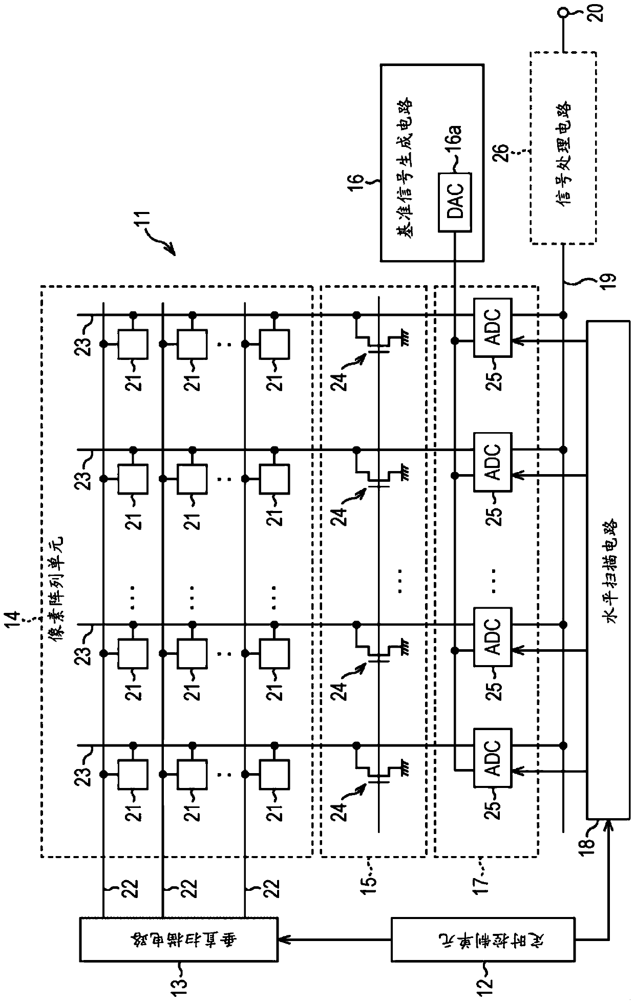
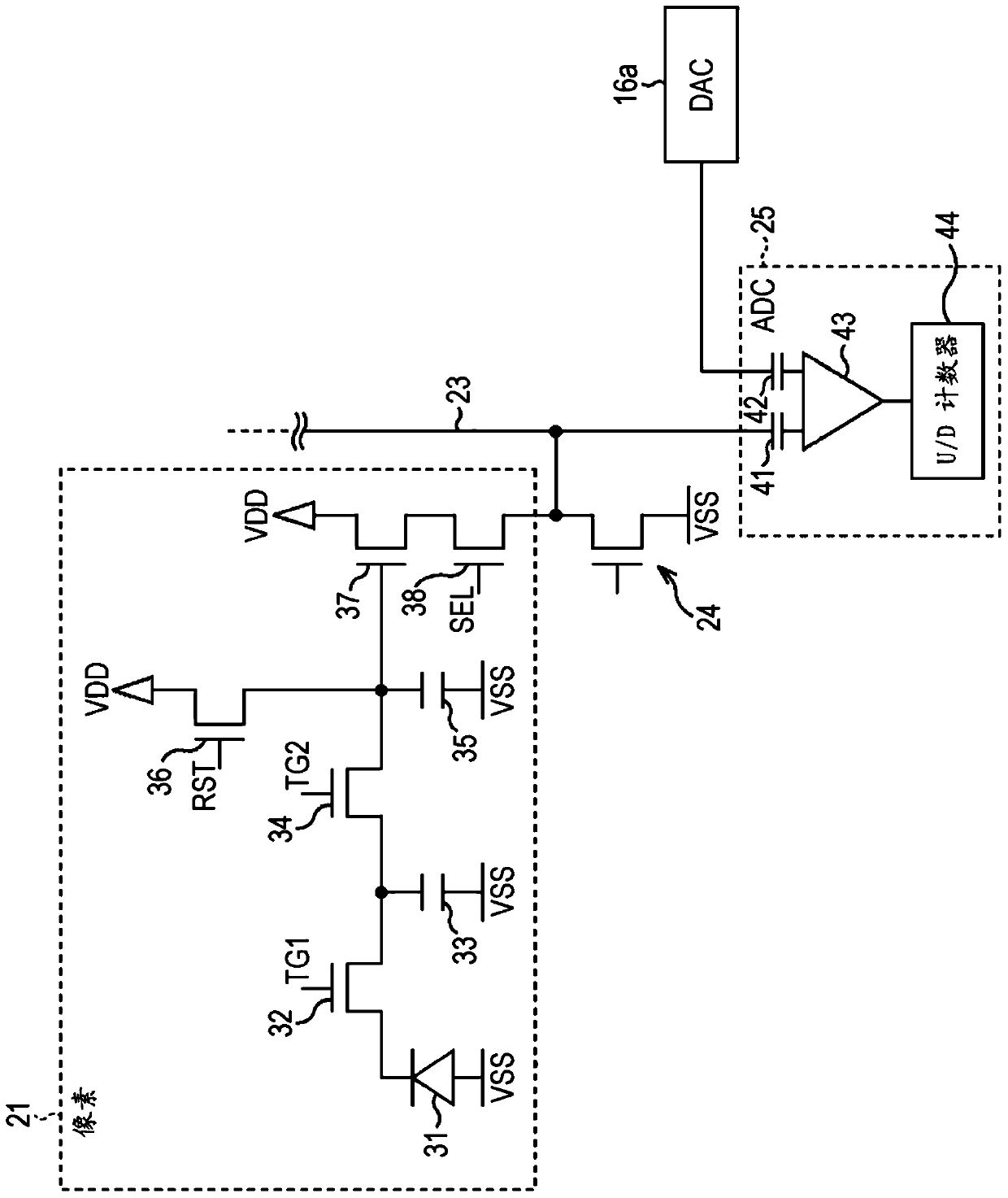
[0031] figure 1 A configuration example of a CMOS image sensor (solid-state imaging device) to which the present technology is applied according to the embodiment is illustrated.

[0032] figure 1 The CMOS image sensor 11 shown in includes a timing control unit 12, a vertical scanning circuit 13, a pixel array unit 14, a constant current source circuit 15, a reference signal generating circuit 16, a column AD converter 17, a horizontal scanning circuit 18, a horizontal output line 19 and output unit 20.

[0033] The timing control unit 12 supplies clock signals and timing signals necessary for predetermined operations to the vertical scanning circuit 13 and the horizontal scanning circuit 18 based on a master clock having a predetermined frequency. For example, the timing control unit 12 supplies timing signals for actuating shutter operations and readout operations of pixels to the vertical scanning circuit 13 and the h...


PUM


Abstract

Solid -state imaging devices, control methods, and electronic equipment. This solid -state imaging device includes: pixel array units with multiple pixels arranged in it, each pixels include at least the photoelectric conversion element corresponding to the charge corresponding to the charge of the light and received the obtained light and keep it.The charged memory generated by the photoelectric conversion element; and the AD conversion unit, which transforms the pixel signal corresponding to the charge from the charger output from pixels to an AD conversion of the count value. Among themThe charge to the memory to keep the charge in the memory, and in the n+1 frame, the first pixel signal corresponding to the charge in the memory and the charge in the memory andThe second pixel signal generated by the charge generated by the photoelectric conversion element, and in the N+1 frame, change the direction of the obtaining counting value between the first and second pixel signals, therebyThe two pixel signals are converted to AD conversion.

Description

technical field [0001] The present technology relates to a solid-state imaging device, a control method, and electronic equipment, and in particular, the present technology relates to a solid-state imaging device capable of outputting a difference between frames, a method for controlling the solid-state imaging device, and electronic equipment including the solid-state imaging device. Background technique [0002] In order to detect a change in an image in a monitoring device or the like, a general method utilizes an inter-frame difference which is a difference between a current image captured at present and an image captured before the current image. Inter-frame difference processing is generally performed by an image processing circuit provided on the downstream side of the image sensor. [0003] An increase in the number of pixels for resolution enhancement of an image sensor increases the data size of a single image and as a result increases the load on image processing....

Claims


Application Information

Patent Timeline
Patent Type & Authority Patents(China)
IPC IPC(8): H04N5/335H04N5/3745H01L27/146H04N25/00
CPCH01L27/14634H04N25/766H04N25/77H04N25/78H04N25/71H04N25/75H04N25/772
Inventor 园田修治
Owner SONY CORP
Features
  • R&D
  • Intellectual Property
  • Life Sciences
  • Materials
  • Tech Scout
  • Unparalleled Data Quality
  • Higher Quality Content
  • 60% Fewer Hallucinations
Learn More