Check patentability & draft patents in minutes with Patsnap Eureka AI!

Memory detection method

A detection method and memory technology, applied in static memory, instruments, etc., can solve the problems of inconsistent data and the inability of memory to work reliably for a long time, and achieve the effect of reducing the probability of non-uniformity

Active Publication Date: 2017-03-29
SHANGHAI HUAHONG GRACE SEMICON MFG CORP
View PDF4 Cites 0 Cited by
  • Summary
  • Abstract
  • Description
  • Claims
  • Application Information

AI Technical Summary

Problems solved by technology

However, using the existing checkerboard test method to check the qualified memory is still unable to work reliably for a long time, and the error that the written data is different from the read data often occurs

Method used


Image

  • Memory detection method
  • Memory detection method
  • Memory detection method

Examples


Embodiment Construction

[0036] In order to make the above objects, features and advantages of the present invention more comprehensible, specific embodiments of the present invention will be described in detail below in conjunction with the accompanying drawings.

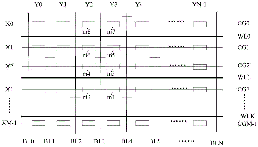
[0037] The memory described in the following embodiments of the present invention can be a FLASH memory, and the specific structure can be found in figure 1 shown.

[0038] Such as figure 1 As shown, the memory includes: memory cells arranged in M ​​rows and N columns, M>1, N>1, and a plurality of bit lines (BL0, BL2, BL3) for selecting the memory cells and providing driving signals , BL4, BL5..., BLN), word lines (WL0, WL1,..., WLK) and control gate lines (CG0, CG1, CG2 and CG3... and CGM-1). The storage unit is M rows and N columns, from row X0, row X1, row X2, row X3... to row XM-1, from column Y0, column Y1, column Y2, column Y3 Column, column Y4... to column YN-1. A storage unit can be a storage bit (bit).

[0039] Each control g...


PUM


Abstract

The invention discloses a method for detecting a memory. The memory comprises storage units arranged in M rows and N lines, wherein M is greater than 1, and N is greater than 1. The method for detecting the memory comprises the following steps: performing first initialization processing on the storage units of M rows and N lines, after the first initialization processing, performing first writing operation on the storage units of M rows and N lines in the sequence from the Mth row of storage units to the first line of storage units, so as to write preset data, after the first writing operation, performing first reading operation on the storage units of M rows and N lines, acquiring first read data according to the comparison result of the reading result of the first reading operation and the result threshold, comparing the first read data with preset data to obtain a first comparison result, and judging and operating the memory according to the first comparison result. By adopting the technical scheme of the invention, the probability that the written data are different from the read data of the memory is further reduced.

Description

technical field [0001] The invention relates to the technical field of semiconductors, in particular to a detection method of a memory. Background technique [0002] With the rapid development of semiconductor technology, mobile storage devices are growing rapidly. As the most commonly used device in mobile storage devices, FLASH chips have been increasingly widely used. In order to ensure the long-term and reliable operation of the FLASH chip, the product needs to be tested at high speed and meticulously before leaving the factory. [0003] figure 1 It is a schematic structural diagram of a memory, which includes: memory cells arranged in a matrix, and a plurality of bit lines (BL0, BL2, BL3, BL4, BL5... , BLN), word lines (WL0, WL1, ..., WLK) and control gate lines (CG0, CG1, CG2 and CG3 ... and CGM-1). The storage unit is M rows and N columns, that is, row X0, row X1, row X2, row X3...row XM-1, and column Y0, column Y1, column Y2, column Y3 , Column Y4...Column YN-1....

Claims


Application Information

Patent Timeline
Patent Type & Authority Patents(China)
IPC IPC(8): G11C29/14
Inventor 张若成顾靖
Owner SHANGHAI HUAHONG GRACE SEMICON MFG CORP
Features
  • R&D
  • Intellectual Property
  • Life Sciences
  • Materials
  • Tech Scout
  • Unparalleled Data Quality
  • Higher Quality Content
  • 60% Fewer Hallucinations
Learn More