Optical device array substrate having a heat dissipating structure integrated with a substrate, and method for manufacturing same

A technology of optical devices and array substrates, which is applied in the direction of electric solid-state devices, semiconductor devices, semiconductor/solid-state device components, etc., can solve problems such as electric shock and short circuit, and achieve the effects of reducing the risk of electric shock, simplifying the process, and smooth ventilation

Inactive Publication Date: 2014-05-07
POINT ENG
View PDF5 Cites 3 Cited by
  • Summary
  • Abstract
  • Description
  • Claims
  • Application Information

AI Technical Summary

Problems solved by technology

[0012] However, due to the structure adopted by this heat sink, the heat dissipation rods of different bodies are connected to the heat dissipation plate as an insulator instead of the conductive substrate itself. Adhesion is still an issue
In addition, since no electrical insulation measures are prepared, a short circuit may occur when a foreign substance is inserted between the cooling rods, and in addition, an electric shock may occur when handling the device while holding the cooling rods

Method used


Image

  • Optical device array substrate having a heat dissipating structure integrated with a substrate, and method for manufacturing same
  • Optical device array substrate having a heat dissipating structure integrated with a substrate, and method for manufacturing same
  • Optical device array substrate having a heat dissipating structure integrated with a substrate, and method for manufacturing same

Examples


Embodiment Construction

[0034] Hereinafter, preferred exemplary embodiments of the present invention, an optical device array substrate with a built-in heat dissipation structure, and a method of manufacturing the same will be described in detail with reference to the accompanying drawings.

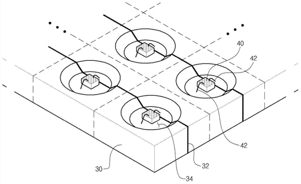
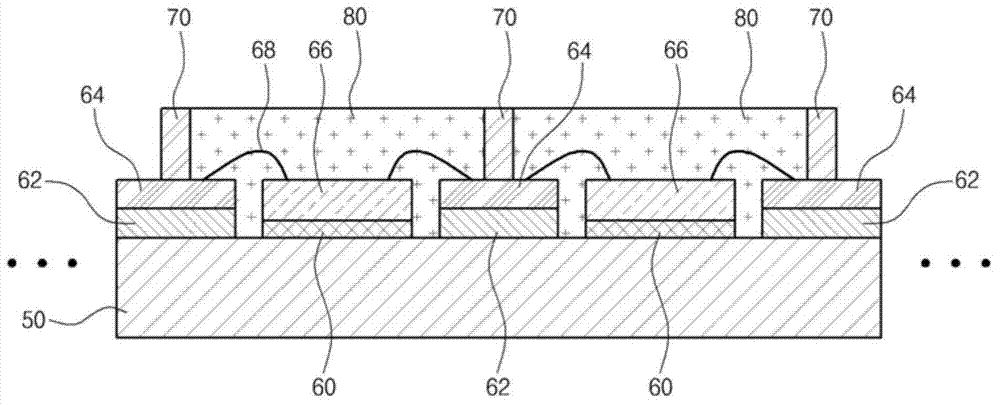
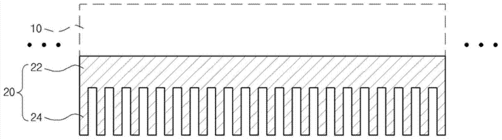
[0035] Figure 4 is a cross-sectional view of an optical device array substrate with a vertical insulating coating in an optical device array substrate with a built-in heat dissipation structure according to an exemplary embodiment of the present invention; for convenience, it is shown to include three columns (with respect to the vertical insulating layer) array of optics. Figure 5 is to show the outline of its bottom surface Figure 4 Partially exploded perspective view of the optics array substrate in . like Figure 4 and 5 As shown, according to the optical device array substrate 100 with a built-in heat dissipation structure of the present invention, in the substrate 100, such as an aluminum or aluminum ...


PUM


Abstract

The present invention relates to an optical device array substrate having a heat dissipating structure integrated with a substrate, and to a method for manufacturing same, wherein the optical device array substrate itself is used as a heat sink and a coupling hole is formed in the bottom of the substrate to have a heat dissipating rod coupled thereto. The optical device array substrate having a heat dissipating structure integrated with a substrate of the present invention consists essentially of: an optical device array substrate having a plurality of optical devices arranged on the top surface thereof and a plurality of coupling holes formed in the bottom surface thereof; and rod-shaped coupling rods that have coupling projections formed on upper ends thereof, and are coupled to each of the coupling holes. In the above-described structure, the coupling holes are formed as screw-coupling holes, and the coupling projections are formed as screw tips so as to be screw-coupled to the coupling holes. The coupling holes are formed having a downwardly narrowing taper, and the coupling projections are formed having a downwardly narrowing taper so as to be precisely coupled with the coupling holes even when in a contracted state under sub-freezing temperatures. The surfaces of the coupling rods are characterized in that insulating coating layers are formed thereon and not on the coupling projections. Further, a portion of the insulating coating layers on some of the coupling rods may be removed to function as electrodes.

Description

technical field [0001] The present invention relates to an optical device array substrate with a built-in heat dissipation structure and a manufacturing method thereof, more particularly, to an optical device array substrate with a built-in heat dissipation structure, wherein the optical device array substrate itself is used as a heat sink, and Coupling holes are formed at the bottom so that the cooling rods can be coupled thereto. Background technique [0002] In general, semiconductor light emitting diodes (LEDs) have received attention from various fields as an environment-friendly light source. Recently, as the application of LEDs has expanded to various fields such as indoor and outdoor lighting, automotive headlights, and backlight units (BLUs) of display devices, high optical efficiency and excellent heat dissipation characteristics are required. For high-efficiency LEDs, it is mainly to improve the material or structure of the LED, however, this requires improving t...

Claims


Application Information

Patent Timeline
Patent Type & Authority Applications(China)
IPC IPC(8): H01L33/64H01L33/48
CPCH01L23/3677H01L23/4006H01L23/4093H01L33/642H01L2224/73265H01L2933/0075H01L33/48H01L33/64H01L33/648
Inventor 安范模南基明全永哲
Owner POINT ENG
Why Eureka
Try Eureka