Electrostatic chuck

a technology of electrostatic chuck and chuck, which is applied in the direction of electrostatic holding devices, manufacturing tools, mechanical apparatuses, etc., can solve the problems of poor thermal coupling between the chuck and the wafer, high energy flux into the wafer, and the possibility of overheating the wafer

Inactive Publication Date: 2000-10-31
SHERMAN ARTHUR
View PDF1 Cites 33 Cited by
  • Summary
  • Abstract
  • Description
  • Claims
  • Application Information

AI Technical Summary

Problems solved by technology

In both of these processes, poor thermal coupling exists between the chuck and wafer due to lack of thermal conduction through a gas between them.
The ion bombardment that occurs in both implantation and etching leads to a high energy flux into the face of the wafer, and the wafer may overheat unless the heat can be removed by heat transfer to the chuck holding it.
Using a cooled chuck will not solve the problem unless some way is found to improve the thermal coupling between the wafer and the chuck.
In general, a wafer ring clamp is undesirable because a clamp covers part of the wafer surface.
Fabricating such a bipolar chuck presents many practical difficulties.
The force of attraction is very sensitive to flatness of the chuck surface, and it is difficult to electrically isolate each half electrode.
Unfortunately, practical semiconductor wafers are more likely to be warped (somewhat like a potato chip) rather than simply bowed.
The Suzuki design offers no solution to this problem.
Even though an electrostatic chuck can hold a wafer in a low pressure reactor, there may still be difficulty in transferring heat into or out of the wafer.
This will not allow adequate control for critical semiconductor processes.
The problem with both of these approaches is undesirably high solid-to-solid thermal contact resistance at low pressures.
Moreover, the invention of Logan is limited to temperatures below 450.degree. C. because of its aluminum construction.
However, consideration was limited to an aluminum...

Method used


Image

  • Electrostatic chuck
  • Electrostatic chuck
  • Electrostatic chuck

Examples


Embodiment Construction

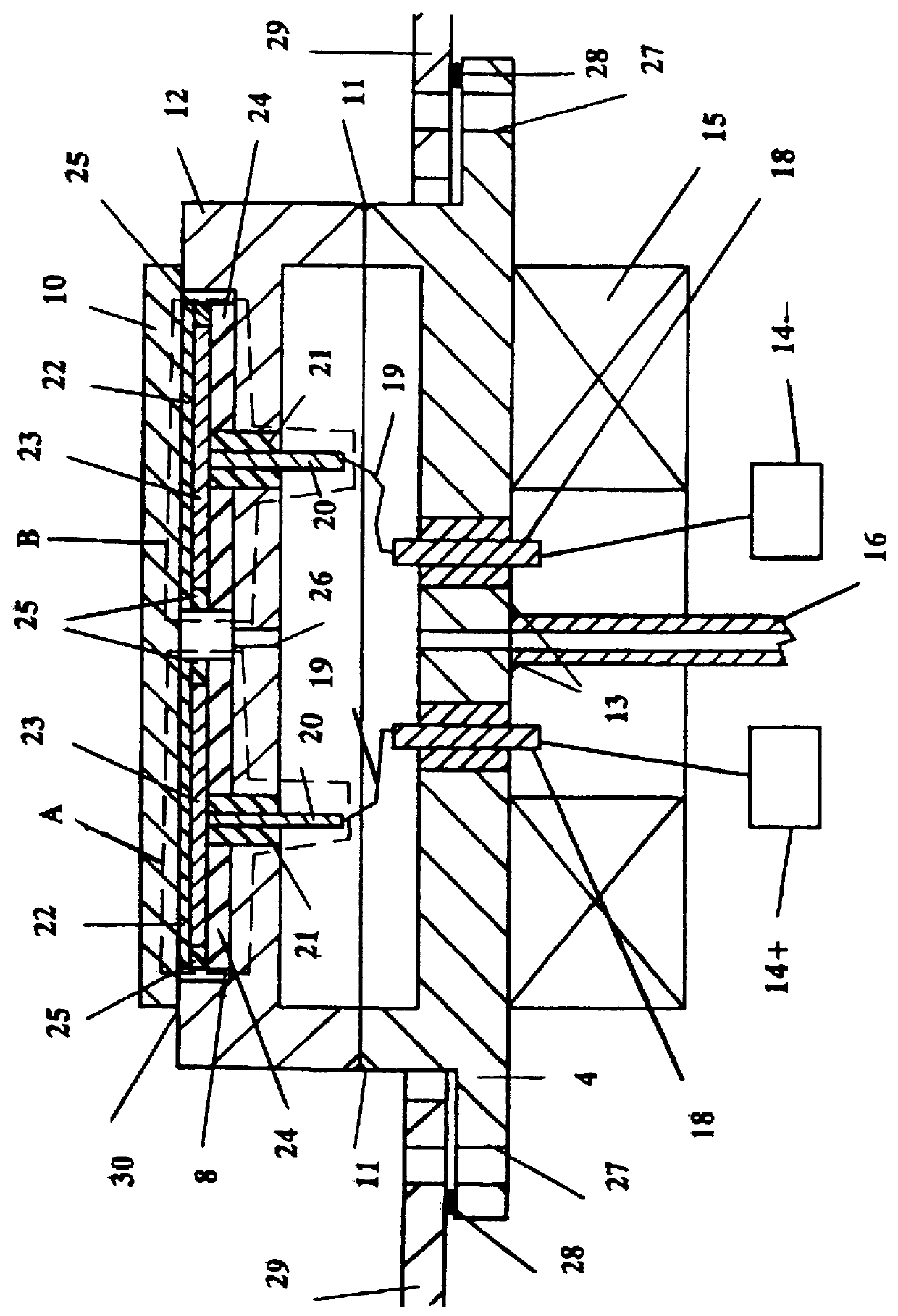
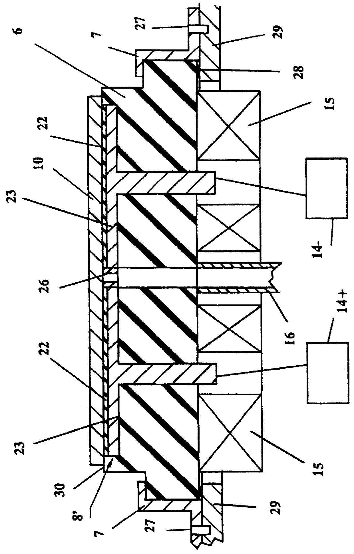
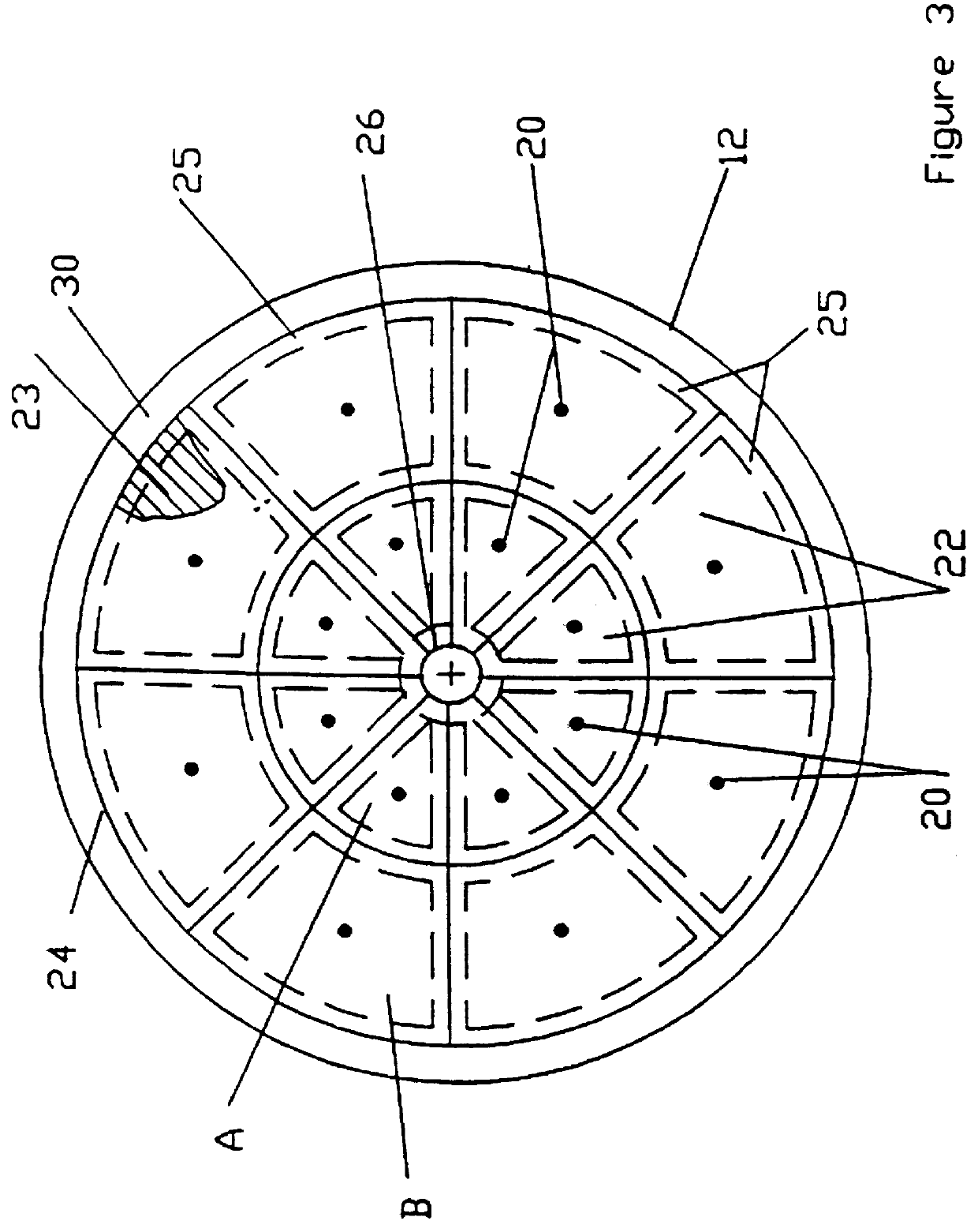
FIG. 1 shows an electrostatic chuck 8 in a metal housing 12, mounted on a reactor chamber wall 29. The chuck 8 has multiple small electrode segments as illustrated in FIGS. 3 and 4. The chuck segments A, B, comprise two thin ceramic plates 22 (the upper plate) and 24 (the lower plate) of suitable refractory dielectric. These two ceramic plates 22 and 24 are separated by, and attached to, a chuck element metal plate 23. Each metal plate 23 has a metal stud 20 attached, so that it can be placed at whatever potential is required, without regard to other chuck elements. Each stud 20 is electrically isolated from the chuck metal base 12 by a dielectric isolator sleeve 21. Each metal plate 23 is further electrically isolated from its environment by the ceramic separators 25, which also serve as a mechanical spacer as hereinafter explained. The chuck metal base 12 is made of a suitable metal and has a circular opening 26 drilled at its center and has a smooth (preferably flat) sealing surf...


PUM


Abstract

An electrostatic chuck is provided having a plurality of small electrostatic structures for holding an electrically conductive workpiece forming a plate of a capacitor. Each electrostatic structure includes a first thermally conductive single-crystal dielectric sheet, and a first electrode in sheet form sandwiched between the first dielectric sheet and a second dielectric surface. The workpiece, typically a conductive or semiconductive wafer, is juxtaposed to the first dielectric sheet of each electrostatic structure and forms a second electrode. The second dielectric sheet, if thick, is used as a thermally conducting base plate which can be attached to a low pressure reactor. If the second dielectric is a thin sheet, then it is mounted to a thermally conductive metal base plate through which heat can be controllably conducted. The resultant electrostatic structure may be brazed to the metal base plate if the thermal expansion characteristics of the two elements are sufficiently matched. The first thermally conductive dielectric sheet is preferably formed of sapphire (Al2O3), which is sufficiently thermally conductive to allow for rapid heat transfer between the base plate and the workpiece. The first electrodes of different electrostatic structures are held at different electrical potentials (typically of several thousand volts difference) and a charge is maintained by this potential difference between selected electrostatic structures.

Description

A. Field of InventionThe present invention pertains to an electrostatic chuck used to hold conducting or semiconducting wafers (such as silicon wafers) in a low pressure or vacuum environment, so that they may be easily cooled or heated. In particular, the present invention relates to the arrangement of high quality materials used, the method of fabrication of a chuck and techniques for operation of a chuck according to the invention.B. Description of Related ArtThere are a number of semiconductor fabrication processes that have to be carried out in a low pressure environment (below one torr). Two that require wafer cooling are ion implantation and reactive ion etching. In both of these processes, poor thermal coupling exists between the chuck and wafer due to lack of thermal conduction through a gas between them. The ion bombardment that occurs in both implantation and etching leads to a high energy flux into the face of the wafer, and the wafer may overheat unless the heat can be ...

Claims


Application Information

Patent Timeline
IPC IPC(8): H01L21/683H01L21/67H01L21/00H02N13/00
CPCH01L21/67103H01L21/6831H02N13/00H01L21/6833Y10T279/23
Inventor SHERMAN, ARTHUR
Owner SHERMAN ARTHUR
Why Eureka
Try Eureka