
Device and operating method for preventing silicon wafer from offset and cracking in cavity transporting process

An operation method and cavity technology, which are applied in semiconductor/solid-state device manufacturing, electrical components, circuits, etc., can solve the problem of position deviation when the robot arm takes the wafer, and it is impossible to detect whether the silicon wafer has shifted or not. Problems such as wafer offset and tilt

Inactive Publication Date: 2014-06-18
SHANGHAI HUAHONG GRACE SEMICON MFG CORP
View PDF5 Cites 2 Cited by
  • Summary
  • Abstract
  • Description
  • Claims
  • Application Information

AI Technical Summary

Problems solved by technology

[0002] In semiconductor equipment, when aluminum is sputtered onto the surface of a silicon wafer at high temperature, the silicon wafer will easily stick to the cavity of the machine in a molten state, causing the position of the mechanical arm to shift when taking the wafer. However, the existing Under the process conditions, after the aluminum film formation is completed, it is transported to other process chambers for film formation, causing silicon wafers to be broken in the chamber, and the cover plate of the chamber (transfer chamber or buffer chamber, etc.) cannot detect the silicon wafer on the conveying arm Whether there is an offset, and it is impossible to detect whether the silicon wafer (wafer) is offset or tilted in the process chamber, which often causes losses

Method used


Image

  • Device and operating method for preventing silicon wafer from offset and cracking in cavity transporting process
  • Device and operating method for preventing silicon wafer from offset and cracking in cavity transporting process
  • Device and operating method for preventing silicon wafer from offset and cracking in cavity transporting process

Examples


Embodiment Construction

[0026] In order to enable your examiners to have a further understanding and understanding of the purpose, features and effects of the present invention, the following detailed description is as follows with the accompanying drawings.

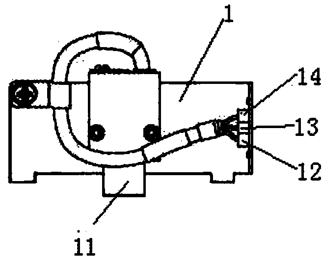
[0027] like figure 1 Shown, be the structure of the photoelectric sensor used in the present invention, comprise measuring port 11 and three interfaces in the photoelectric sensor 1, described three interfaces are respectively photoelectric sensor positive input end 12, photoelectric sensor negative input end 13 and photoelectric sensor Sensor signal terminal 14.

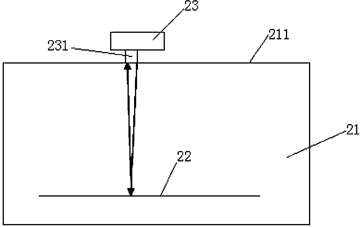
[0028] like figure 2 As shown, it is a schematic diagram of the position measurement of the photoelectric sensor of the present invention. A light beam is emitted from the measurement port 231 of the photoelectric sensor 23 to the surface of the silicon wafer 22 to be measured, and the measurement port 231 is emitted from the surface of the silicon wafer 22, thereby measuring the p...


PUM


Abstract

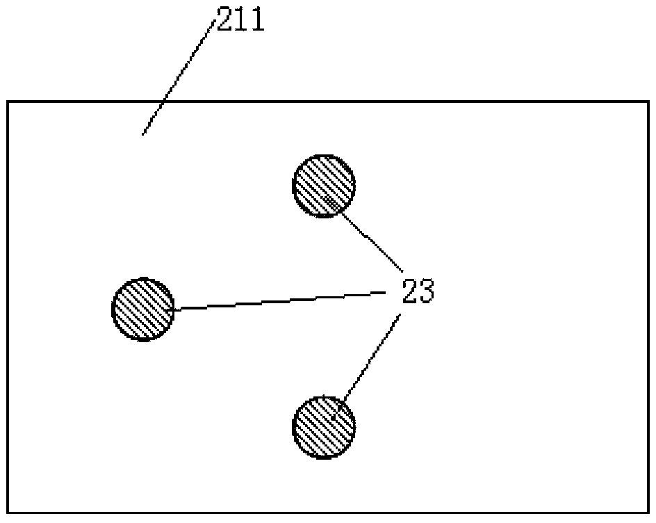
The invention discloses a device for preventing a silicon wafer from offset and cracking in a cavity transporting process. The device comprises a cavity, at least three photoelectric sensors, a control device and a manipulator, a top cover of the cavity is made of transparent material; the photoelectric sensors are not on a straight line and fixedly installed on the top cover of the cavity, signal ends of the at least three photoelectric sensors are connected in series to the control device, the control device is connected with the manipulator, and the silicon wafer is moved through the manipulator. The device in the invention can accurately monitor the position of the silicon wafer, and once offset of the silicon wafer is monitored, the device performs braking and gives an alarm in time, thereby preventing the silicon wafer from being cracked up or entering the cavity with offset and causing abnormal film formation.

Description

technical field [0001] The invention relates to a semiconductor integrated circuit manufacturing process equipment, in particular to a device for preventing silicon wafers from shifting fragments during cavity conveyance, and also relates to an operation method of the device. Background technique [0002] In semiconductor equipment, when aluminum is sputtered onto the surface of a silicon wafer at high temperature, the silicon wafer will easily stick to the cavity of the machine in a molten state, causing the position of the mechanical arm to shift when taking the wafer. However, the existing Under the process conditions, after the aluminum film formation is completed, it is transported to other process chambers for film formation, causing the silicon wafers to be broken in the chamber, and the cover plate of the chamber (transfer chamber or buffer chamber, etc.) cannot detect the silicon wafer on the conveying arm Whether there is an offset, and it is impossible to detect w...

Claims


Application Information

Patent Timeline
Patent Type & Authority Applications(China)
IPC IPC(8): H01L21/67
CPCH01L21/67265
Inventor 龚晓丹张嘉训周捷
Owner SHANGHAI HUAHONG GRACE SEMICON MFG CORP
Learn More