Manufacturing system of optical display device and manufacturing method
What is Al technical title?
Al technical title is built by PatSnap Al team. It summarizes the technical point description of the patent document.
An optical display and production system technology, applied in optics, nonlinear optics, instruments, etc., can solve problems such as poor bonding and easy adhesion of dust, and achieve miniaturization of equipment, suppression of poor bonding, and suppression of scratches or Effect of adhesion of foreign matter
Active Publication Date: 2014-07-02
SUMITOMO CHEM CO LTD
View PDF6 Cites 5 Cited by
Summary
Abstract
Description
Claims
Application Information
AI Technical Summary
This helps you quickly interpret patents by identifying the three key elements:
Problems solved by technology
Method used
Benefits of technology
Problems solved by technology
[0009] Again, before the optical member is bonded to the liquid crystal panel, dust is suppressed from adhering to the liquid crystal panel by static electricity removal of the liquid crystal panel, etc., but there is also the following problem: since the bonding surface of the optical member bonded to the liquid crystal panel has Adhesive, so dust is easy to adhere to, which becomes a cause of poor bonding
Method used
Image
Click on the blue label to locate the original text in one second.
Reading with bidirectional positioning of images and text.
Examples
no. 1 approach
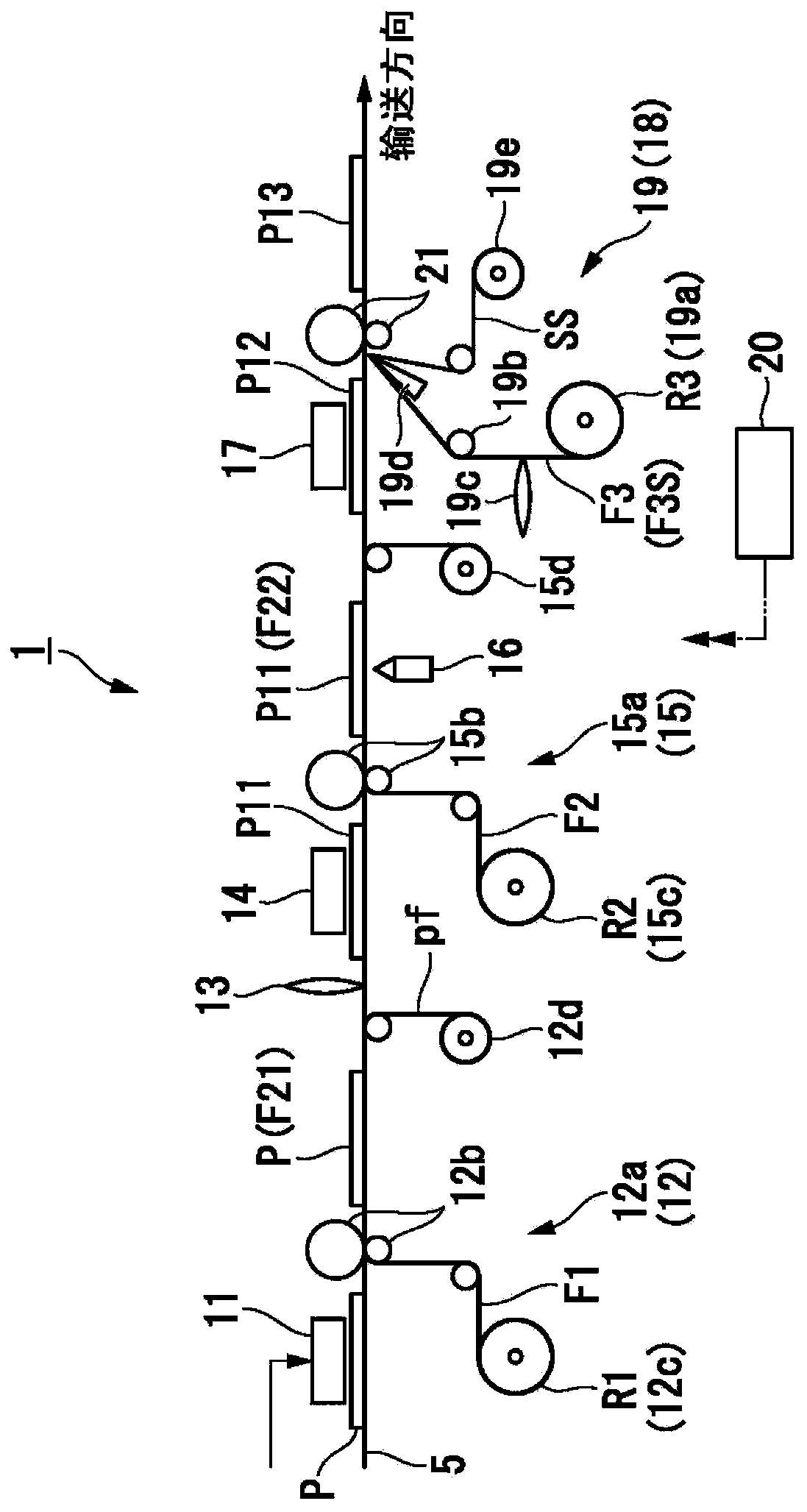
[0041] Hereinafter, a first embodiment of the present invention will be described with reference to the drawings. In this embodiment, as a production system of an optical display device, a film bonding system constituting a part thereof will be described.
[0042] In particular, as described in detail below, in the film bonding system of the first embodiment, the bonding devices 12, 15, 18 are arranged under the roller conveyor 5, and the cutting device 13 is arranged under the roller conveyor 5. Machine 5 above.
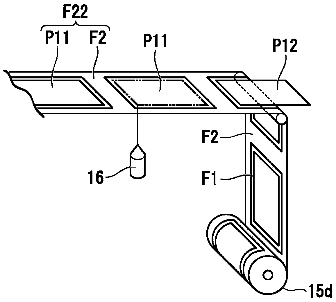
[0043] figure 1 It shows the schematic structure of the film bonding system 1 of this embodiment. The film bonding system 1 bonds film-shaped optical members such as polarizing films, retardation films, and brightness enhancement films to panel-shaped optical display components such as liquid crystal panels and organic EL panels. The film bonding system 1 manufactures the optical member bonding body containing the said optical display component and an optical mem...
no. 2 approach
[0120] Hereinafter, a second embodiment of the present invention will be described with reference to the drawings. In this embodiment, as a production system of an optical display device, a film bonding system constituting a part thereof will be described.
[0121] In the second embodiment, the same symbols are assigned to the same components as those in the first embodiment, and descriptions thereof are omitted or simplified.
[0122] In particular, as described in detail below, in the film bonding system of the first embodiment, the bonding devices 112, 115, 118 are arranged on the roller conveyor 105, and the cutting device 113 is arranged on the roller conveyor. Machine 105 under.
[0123] Figure 13 It shows the schematic structure of the film bonding system 101 of this embodiment. The film bonding system 101 bonds a film-shaped optical member such as a polarizing film, a retardation film, or a brightness enhancement film to a panel-shaped optical display component suc...
PUM
Abstract
A manufacturing system of an optical display device of the present invention is a manufacturing system of an optical display device that bonds an optical material to an optical display component and is provided with a primary bonding device that bonds a first surface of a plurality of optical display components to the primary optical material sheet while unwinding a band-shaped primary optical sheet from a primary whole roll where the sheet has a larger width than the width of the display region of an optical display component in the width direction of the component perpendicular to the transport direction of the optical display components for a plurality of optical display components transported on a line; a primary cutting device that cuts out a primary optical bonding body that includes a single optical display component and the primary optical material overlapping the single optical display component from a bonding sheet by cutting the part opposite the primary optical component sheet facing the display region and the remaining part positioned on the outside of the opposite part, and cuts out the primary optical material as the optical material having a size corresponding to the display region from the primary optical component sheet; and a secondary bonding device that bonds secondary optical parts to the second surfaces of the optical display components in the bonding part of the primary optical bonding material while transporting the plurality of secondary optical materials with a separator sheet as the carrier after the band-shaped secondary optical component sheet having a width corresponding to the display region in the width direction of a component for a plurality of bonding bodies of primary optical parts transported on the line is wound out together with the separator sheet from the secondary whole roll; cutting is performed along the width direction each time the secondary optical component sheet is unrolled to the length corresponding to the display region in the secondary optical component sheet; and the secondary optical materials are formed as optical parts having sizes corresponding to that of the display region.
Description
technical field [0001] The present invention relates to a production system and production method of optical display devices such as liquid crystal displays. [0002] The present invention claims priority based on Japanese Patent Application No. 2011-262949 filed on November 30, 2011 and Japanese Patent Application No. 2011-262950 filed on November 30, 2011, the contents of which are incorporated herein. Background technique [0003] Conventionally, in the production system of optical display devices such as liquid crystal displays, optical members such as polarizers bonded to liquid crystal panels (optical display components) are cut from long films into sheets of the size corresponding to the display area of the liquid crystal panel. , is packaged and transported to another production line, and then bonded to a liquid crystal panel (for example, refer to Patent Document 1). [0004] prior art literature [0005] patent documents [0006] Patent Document 1 Japanese Pat...
Claims
Application Information
Patent Timeline
Application Date:The date an application was filed.
Publication Date:The date a patent or application was officially published.
First Publication Date:The earliest publication date of a patent with the same application number.
Issue Date:Publication date of the patent grant document.
PCT Entry Date:The Entry date of PCT National Phase.
Estimated Expiry Date:The statutory expiry date of a patent right according to the Patent Law, and it is the longest term of protection that the patent right can achieve without the termination of the patent right due to other reasons(Term extension factor has been taken into account ).
Invalid Date:Actual expiry date is based on effective date or publication date of legal transaction data of invalid patent.