Supercharge Your Innovation With Domain-Expert AI Agents!

Function switching circuit applicable to chip testing

A technology of function switching and chip testing, which is applied in the direction of electrical components, code conversion, parallel/serial conversion, etc., can solve the problems of high comprehensive cost of traditional solutions, achieve the effects of increased flexibility, simple implementation, and small circuit area

Active Publication Date: 2014-07-09
XI AN UNIIC SEMICON CO LTD
View PDF5 Cites 0 Cited by
  • Summary
  • Abstract
  • Description
  • Claims
  • Application Information

AI Technical Summary

Problems solved by technology

[0005] In order to solve the problem of high comprehensive cost of traditional solutions, the present invention proposes a new function switching circuit suitable for chip testing

Method used


Image

  • Function switching circuit applicable to chip testing
  • Function switching circuit applicable to chip testing
  • Function switching circuit applicable to chip testing

Examples


Embodiment 1

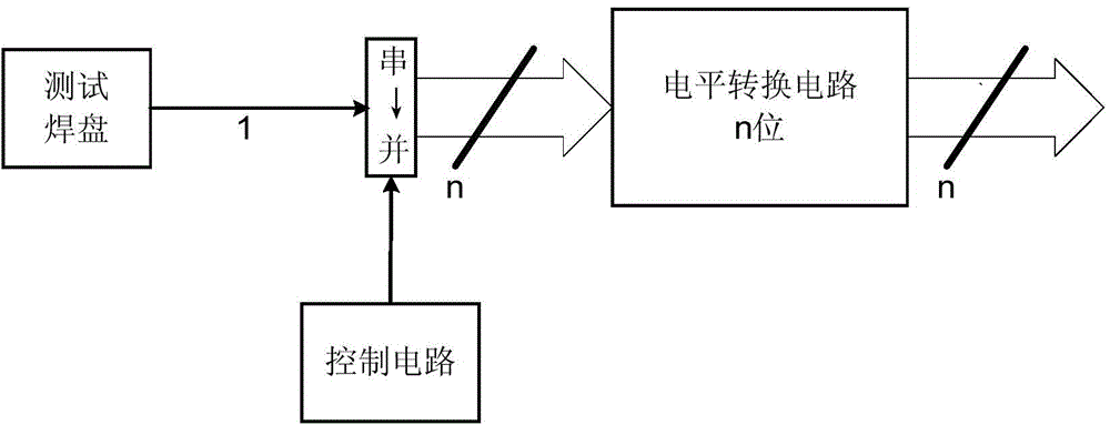
[0022] Such as figure 2 As shown, the original n-bit fuse circuit is changed to a 1-bit test pad, connected to a serial → parallel conversion circuit (serial to parallel). Through the serial→parallel conversion circuit, the 1-bit serial signal is converted into an n-bit parallel signal, and the n-bit parallel signal passes through the n-bit level conversion circuit, which can realize conversion output at various levels for other circuits. Correspondingly, an additional control circuit needs to be set up to control the serial→parallel conversion circuit.

[0023] Such as Figure 4 As shown, the present invention provides a basic structure of the control circuit. The main function of the control circuit is to control the working state of the serial→parallel conversion circuit. It includes a logic circuit, a clock circuit and a counting circuit, and the logic circuit controls the clock circuit and the counting circuit.

[0024] Assume that the serial conversion here only nee...

Embodiment 2

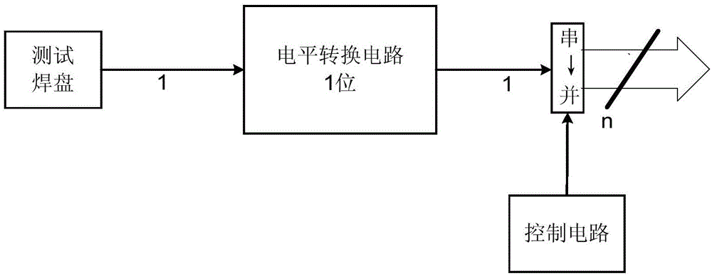
[0031] Such as image 3 As shown, the original n-bit fuse circuit is changed to a test pad, connected to a 1-bit level conversion circuit to convert the signal to the set level, and then output n-bit parallel signals through the serial→parallel conversion circuit. Correspondingly, an additional control circuit needs to be set up to control the serial→parallel conversion circuit.

[0032] Specific examples of the control circuit and the serial→parallel conversion circuit can be implemented with reference to the first embodiment above.


PUM


Abstract

The invention provides a function switching circuit applicable to chip testing. The function switching circuit applicable to chip testing mainly comprises a testing bonding pad, a serial-to-parallel converting circuit, a control circuit and an n-bit electrical level converting circuit. The control circuit is used for controlling the serial-to-parallel converting circuit so that a one-bit electrical level signal output by the testing bonding pad can be converted into an m-bit-parallel signal by the serial-to-parallel converting circuit, wherein m is smaller than or equal to n. Finally, the m-bit-parallel signal is output after being subjected to conversion through an m-bit electric level in the n-bit electrical level converting circuit. According to the function switching circuit applicable to chip testing, a traditional fuse wire circuit is replaced by the testing bonding pad, different signals can be input by inserting an external probe into the testing bonding pad, and the function of the n-bit fuse wire circuit in the prior art can be achieved through only one testing bonding pad.

Description

technical field [0001] The invention relates to a function switching circuit suitable for chip testing. Background technique [0002] In the design and manufacture of chips, fuse circuits are often used. The main function of the fuse is: after the production of the chip is completed, the fuse needs to be switched according to the test results or function settings. A change in connection that changes the working state or function of a circuit. [0003] Due to different working power sources, the output signal of the fuse circuit cannot be directly used by the circuit. The signal of the fuse circuit needs to be processed by the level conversion circuit before being output to other circuits for use. Usually, each bit of fuse circuit is connected to a bit of level conversion circuit. Such as figure 1 As shown, it is the fuse circuit structure in the prior art, and the n-bit fuse circuit in the figure is used in conjunction with the n-bit level conversion circuit. [0004] ...

Claims


Application Information

Patent Timeline
Patent Type & Authority Applications(China)
IPC IPC(8): H03M9/00
Inventor 李晓骏
Owner XI AN UNIIC SEMICON CO LTD
Features
  • R&D
  • Intellectual Property
  • Life Sciences
  • Materials
  • Tech Scout
  • Unparalleled Data Quality
  • Higher Quality Content
  • 60% Fewer Hallucinations
Learn More