

Composite dielectric grating metal-oxide-semiconductor field effect transistor (MOSFET) based dual-transistor light-sensitive detector and signal reading method thereof
A photosensitive detector and dual transistor technology, applied in image communication, color TV parts, TV system parts, etc., can solve the problems of low sensitivity and resolution, and achieve the effect of avoiding mutual interference
- Summary
- Abstract
- Description
- Claims
- Application Information
AI Technical Summary
Problems solved by technology
Method used
Image

Examples
Embodiment Construction
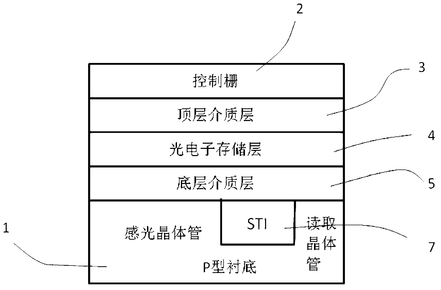
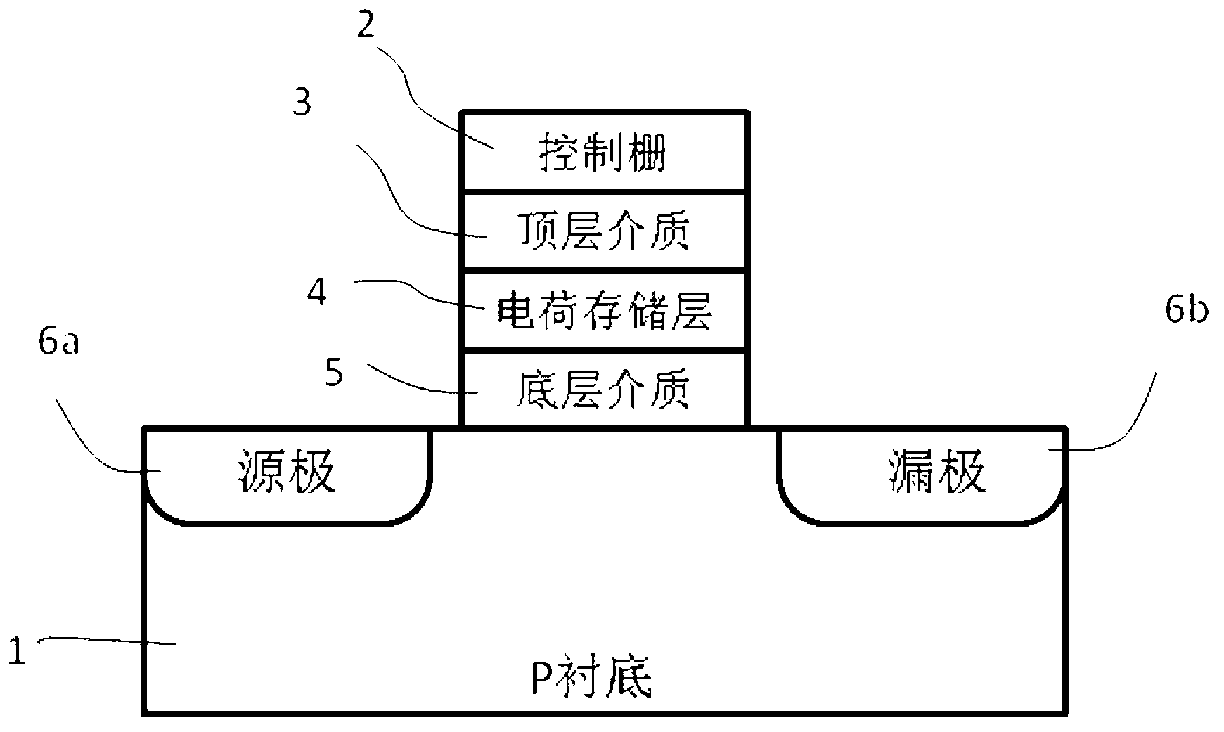
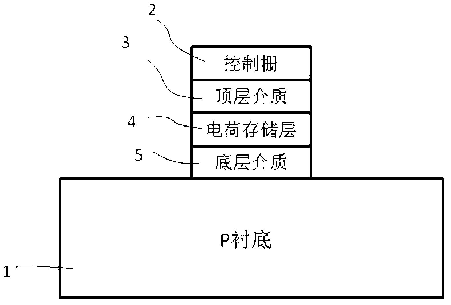
[0029] Double-transistor photosensitive detector single-tube structure (such as Figure 1-Figure 3 ), consisting of two transistors (a phototransistor and a readout transistor) form a basic unit of a photodetector. Structures include:
[0030] A semiconductor substrate (P-type) 1; a bottom insulating medium 5, an optoelectronic storage layer 4, a top insulating medium 3, and a control gate 2 are sequentially arranged directly above the semiconductor substrate; in the semiconductor substrate 1 (on the read transistor side), N-type source 6 a and drain 6 b are formed by ion implantation doping; the two transistors are isolated by shallow trench isolation 7 . The charge storage layer 4 is polysilicon, Si 3 N 4 Or other electronic conductors or semiconductors; the control grid 2 is polysilicon, metal or transparent conductive electrode, and at least one of the control grid surface or base layer is a window that is transparent or translucent to the detection wavelength of the de...
PUM
 Abstract
Description
Claims
Application Information