
Method for measuring electric leakage of PMOS device

A measurement method and device technology, applied in semiconductor/solid-state device testing/measurement, circuits, electrical components, etc., can solve problems such as increase and inaccurate test data

Active Publication Date: 2014-08-20
SHANGHAI HUALI MICROELECTRONICS CORP
View PDF6 Cites 2 Cited by
  • Summary
  • Abstract
  • Description
  • Claims
  • Application Information

AI Technical Summary

Problems solved by technology

At this time, the leakage current IB measured at the body region end contact region 50 will increase, resulting in inaccurate test data.

Method used


Image

  • Method for measuring electric leakage of PMOS device
  • Method for measuring electric leakage of PMOS device
  • Method for measuring electric leakage of PMOS device

Examples


Embodiment Construction

[0016] In order to make the content of the present invention clearer and easier to understand, the content of the present invention will be described in detail below in conjunction with specific embodiments and accompanying drawings.

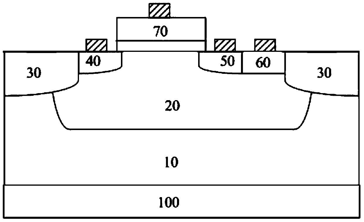
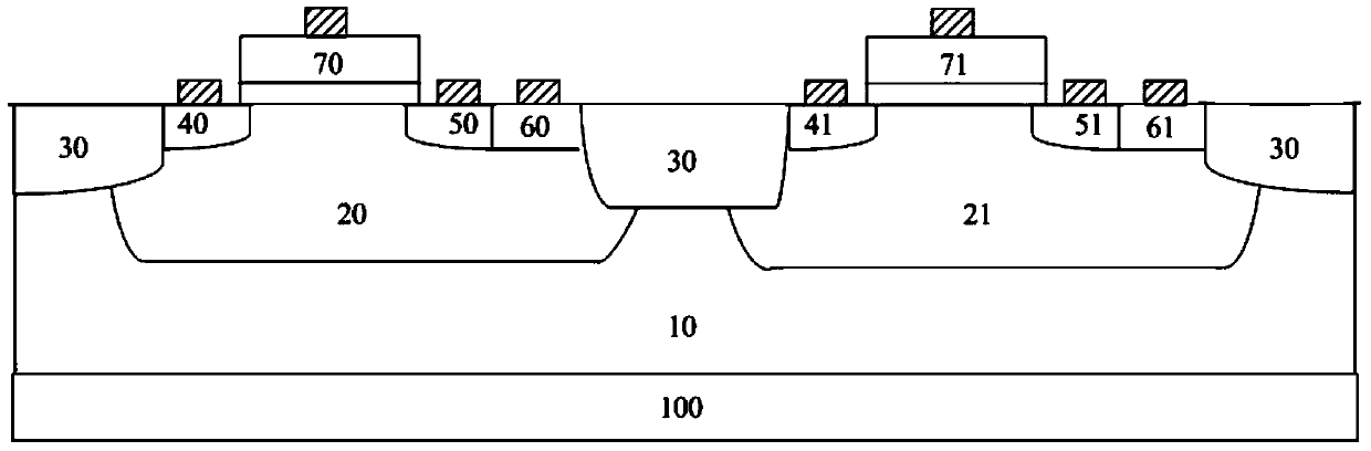
[0017] image 3 It schematically shows a leakage measurement structure of a PMOS device according to a preferred embodiment of the present invention.

[0018] Such as image 3 As shown, the PMOS device leakage measurement method according to a preferred embodiment of the present invention includes:

[0019] A wafer formed with a CMOS device is placed on a test tray 100, wherein the CMOS device includes a paired PMOS device and an NMOS device formed on the same substrate 10; and the PMOS device includes an N well formed in the substrate 10 20 in the P-type drain 40, P-type source 50 and N-type body contact region 60, the PMOS device also includes a base 70 formed on the substrate 10; the NMOS device includes a P well formed in the substrate 10 ...


PUM


Abstract

The invention provides a method for measuring an electric leakage of a PMOS device. The method comprises the steps that a wafer with a formed CMOS device is placed on a test tray, wherein the CMOS device comprises the PMOS device and an NMOS device which are formed on the same substrate in pair, the PMOS device comprises a P-type drain electrode, a P-type source electrode and an N-body contact zone, the P-type drain electrode, the P-type source electrode and the N-body contact zone are formed in an N-well in the substrate, the NMOS device comprises an N-type drain electrode, an N-type source electrode and a P-body contact zone, the N-type drain electrode, the N-type source electrode and the P-body contact zone are formed in an P-well in the substrate, and the N-well is electrically isolated from the P-well through an isolation zone; under the condition that the voltage exerted on the contact zone of the NMOS device is identical to the voltage exerted on the N-body contact zone, electric leakage measurement is conducted on the PMOS device. By the adoption of the method for measuring the electric leakage of the PMOS device, under the condition that the layout of an existing CMOS device is not changed, the problem that when the PMOS is in the switched-off state, the electric leakage is large is solved, the utilization efficiency of the device is improved, the occupied area of the layout is reduced, and the purpose of cost reduction is achieved.

Description

technical field [0001] The present invention relates to the WAT test (wafer acceptance test, wafer acceptability test) of CMOS semiconductor device, more specifically, the present invention relates to a kind of leakage measurement method of PMOS device. Background technique [0002] With the development of CMOS semiconductor device technology and the proportional size reduction, it is necessary to consider the power consumption of the system standby when designing, and it is necessary to reduce the off-state leakage of CMOS devices. Accurate measurement data is the foundation of process development. [0003] WAT (wafer acceptance test, wafer acceptability test) refers to testing the test key (testkey) in the dicing line after the entire wafer is manufactured, but before packaging. The WAT test is an electrical test performed on various test structures on the semiconductor silicon wafer after completing all the manufacturing processes. Through the analysis of WAT data, prob...

Claims


Application Information

Patent Timeline
IPC IPC(8): H01L21/66
CPCH01L22/14
Inventor 杜宏亮
Owner SHANGHAI HUALI MICROELECTRONICS CORP
Learn More