Semiconductor chips and semiconductor devices

A semiconductor and chip technology, applied in the direction of semiconductor devices, semiconductor/solid-state device manufacturing, semiconductor/solid-state device components, etc., can solve problems such as increased wiring impedance, decreased wiring performance, and increased size

Inactive Publication Date: 2018-04-13
RENESAS ELECTRONICS CORP
View PDF12 Cites 0 Cited by
  • Summary
  • Abstract
  • Description
  • Claims
  • Application Information

AI Technical Summary

Problems solved by technology

For example, the via hole cannot be placed near the substrate pad to be connected to it, and the lead-out of the wiring from the substrate pad to the via hole increases, the wiring impedance increases, and the electrical characteristics deteriorate.
In addition, the wiring performance on the layout surface is reduced, the area of ​​the substrate is increased, and, for example, when the substrate is a mounting substrate of an LSI package, there are problems such as an increase in the size of the package that can be accommodated.

Method used


Image

  • Semiconductor chips and semiconductor devices
  • Semiconductor chips and semiconductor devices
  • Semiconductor chips and semiconductor devices

Examples


Embodiment approach 1

[0206] [Embodiment 1]

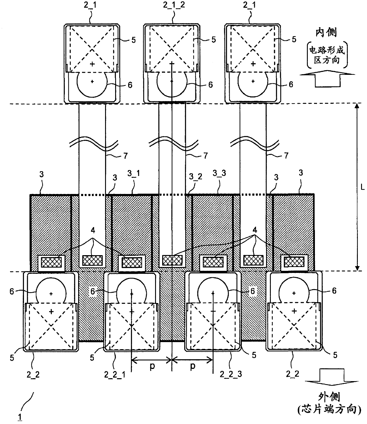
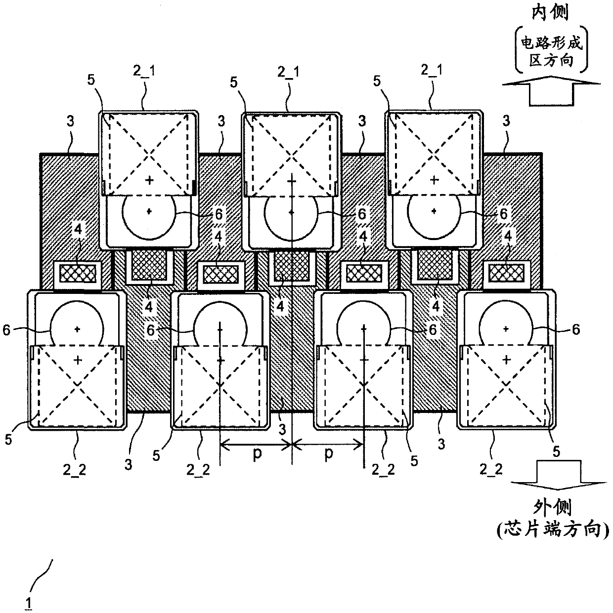
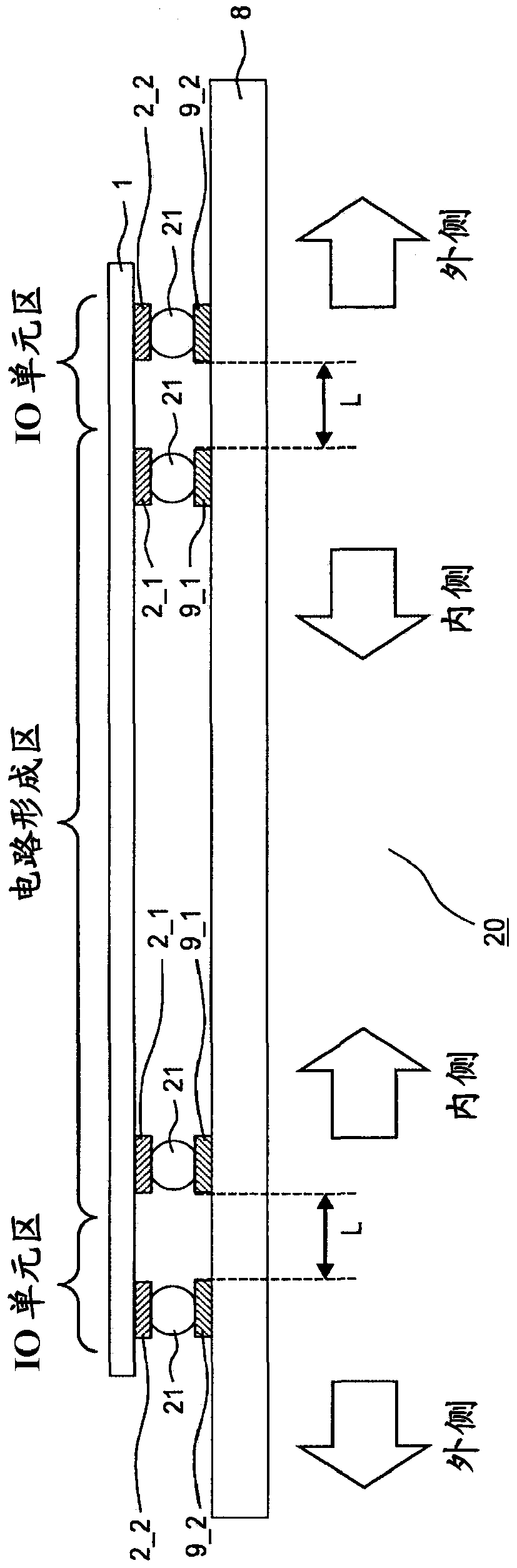
[0207] figure 1 is a layout diagram showing the arrangement of the pads 2 in the semiconductor chip 1 of Embodiment 1, figure 2 It is a layout diagram showing the arrangement of pads in a conventional semiconductor chip. image 3 It is a schematic diagram showing the mounting state in the cross-sectional direction of the semiconductor device 20 in which the semiconductor chip 1 of Embodiment 1 is flip-chip mounted on the substrate 8, Figure 4 It is a schematic diagram showing the arrangement of the pads 2 in the semiconductor chip 1 of Embodiment 1 and Embodiment 2 and the arrangement of the substrate pads 9 in the substrate 8 on which it is flip-chip mounted.

[0208] The semiconductor device 20 of the first embodiment is like image 3 As shown, a semiconductor chip 1 is flip-chip mounted on a substrate 8 to form a configuration. The semiconductor chip 1 has die pads 2_1 and 2_2 ; the substrate 8 has substrate pads 9_1 and 9_2 respect...

Embodiment approach 2

[0225] [Embodiment 2]

[0226] For the prescribed method for the predetermined distance L, reference Figure 9 Description and Reference Figure 5 The illustrated example differs from the example. The same applies to the predetermined distance L in consideration of the wiring properties in the substrate 8 on which the semiconductor chip 1 is flip-chip mounted, but it is also specified in consideration of the wiring properties of the plated wiring.

[0227] Other configurations are the same as those described in Embodiment 1. against figure 1 , image 3 , Figure 4 The descriptions above are also applicable to Embodiment 2.

[0228] Figure 9 It is a layout diagram showing the arrangement of substrate pads 9_1 and 9_2 in substrate 8 on which semiconductor chip 1 of Embodiment 2 is flip-chip mounted.

[0229] In the substrate 8, an inner substrate pad row consisting of a plurality of substrate pads 9_1 connected to the inner pad row of the semiconductor...

Embodiment approach 3

[0233] [Embodiment 3]

[0234] Embodiments 1 and 2 show an example in which the probe region 5 and the bonding region 6 are provided on the same die pad. Here, since the probing area 5 is used to apply a test signal or observe an output signal in the test of the semiconductor chip 1 as described above, and is used for contact with the probe, it is pressed against the probe during the test. while applying pressure. In the conventional semiconductor chip, it can be arranged in the area of ​​the input / output unit 3 or on the gap area with the internal circuit, so the pressing by the probe does not affect the internal circuit. However, as described in Embodiments 1 and 2, since the inner pad row is moved toward the inner side, that is, toward the circuit formation region, there is a possibility that the inner pad row is arranged on the internal circuit. In this case, the pressure by the probe affects the characteristics and operation of the internal circuit, making it diffi...


PUM


Abstract

Provided are a semiconductor chip and a semiconductor device that improve wiring properties in a substrate on which a semiconductor chip is flip-chip mounted. In the flip-chip mounted semiconductor chip, the inner die pad row and the outer die pad row arranged in a zigzag shape inside and outside the IO cell are arranged at a predetermined interval or more. The predetermined interval is an interval at which one via hole can be disposed between the inner and outer substrate pad rows on the substrate that are connected face-to-face with the inner and outer chip pad rows. Alternatively, the predetermined interval means an interval at which an opening for wiring a solder resist layer to which a plated line is to be back-etched later can be formed at the interval. Even when there is no space for forming wiring between the outer substrate pad columns, the wiring property of the substrate can be improved.

Description

technical field [0001] The present invention relates to a semiconductor chip flip-chip mounted on a substrate and a semiconductor device mounted thereon, and is particularly applicable to improving the wiring properties of the mounted substrate. Background technique [0002] In flip-chip mounting, on a substrate on which a semiconductor chip is mounted, pads to be connected are provided at positions facing the pads of the semiconductor chip, and are connected to each other via bumps or the like to achieve electrical conduction. Hereinafter, pads provided on a substrate for connection to a semiconductor chip are referred to as substrate pads, and pads on the semiconductor chip are simply referred to as pads or die pads. [0003] In semiconductor chips, especially with the increase in the integration level of large-scale LSI (Large Scale Integrated circuit, large-scale integrated circuit) such as SoC (System on Chip), there is a need for more electrodes, that is, the number of...

Claims


Application Information

Patent Timeline
Patent Type & Authority Patents(China)
IPC IPC(8): H01L23/488H01L25/16
CPCH01L25/0657H01L2224/16225H01L2224/32145H01L2224/48227H01L2224/48464H01L2224/73265H01L2225/0651H01L2225/06517H01L2924/15311H01L2225/06558H01L23/04H01L23/49838H01L21/563H01L24/73H01L23/49816H01L2924/00012H01L23/12H01L24/17
Inventor 棈松高志別井隆文黒田淳
Owner RENESAS ELECTRONICS CORP
Why Eureka
Try Eureka