Packaging method for organic light-emitting display panel and organic light-emitting display panel

An encapsulation method and a light-emitting display technology, which are applied in the directions of organic semiconductor devices, electrical components, and electric solid-state devices, etc., can solve problems such as difficulty in realizing a narrower frame design.

Active Publication Date: 2016-01-06
BOE TECH GRP CO LTD
View PDF8 Cites 0 Cited by
  • Summary
  • Abstract
  • Description
  • Claims
  • Application Information

AI Technical Summary

Problems solved by technology

[0007] The mask plate and ALD technology are used to coat the substrate on which the OLED is formed. The film wrapping (StepCoverage) formed by the ALD technology is better, and the area of ​​the film layer formed on the substrate corresponding to the hollow area of ​​the mask plate is larger than the area of ​​the hollow area. For example, in general, the film wrapping range formed by ALD technology is about 5-10 mm, and the distance between the terminal electrode and the edge of the film package obtained by traditional mask technology is about 5-20 mm, making it difficult to achieve a narrower frame design

Method used


Image

  • Packaging method for organic light-emitting display panel and organic light-emitting display panel
  • Packaging method for organic light-emitting display panel and organic light-emitting display panel
  • Packaging method for organic light-emitting display panel and organic light-emitting display panel

Examples


Embodiment approach

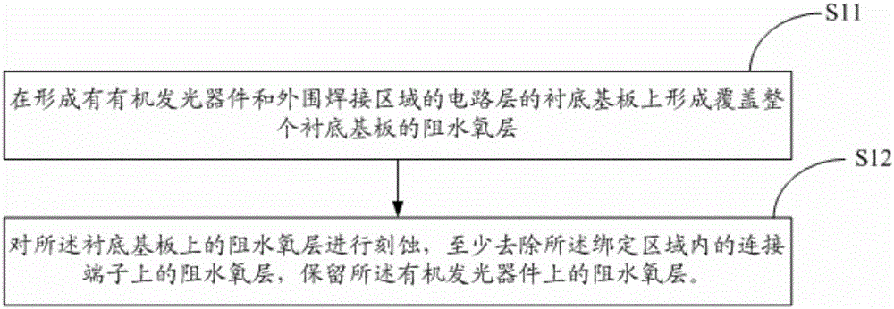
[0042] Method 1: remove all water and oxygen blocking layers in the binding area;

[0043] Method 2: remove the water-blocking oxygen layer on the connection terminals in the binding area, that is, retain the water-blocking oxygen layer outside the connection terminals.

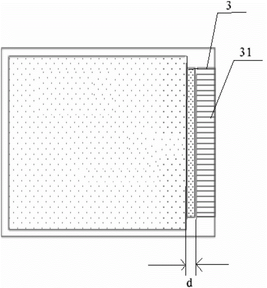
[0044] The size and setting position of the binding area of ​​the organic light-emitting display panel are determined according to actual needs, for example, as figure 2 As shown, the size of the binding area 3 of the organic light emitting display panel may be equivalent to the area covered by the connection terminal 31 . The binding area 3 is located at an area extending a certain distance from the edge of the substrate to the center.

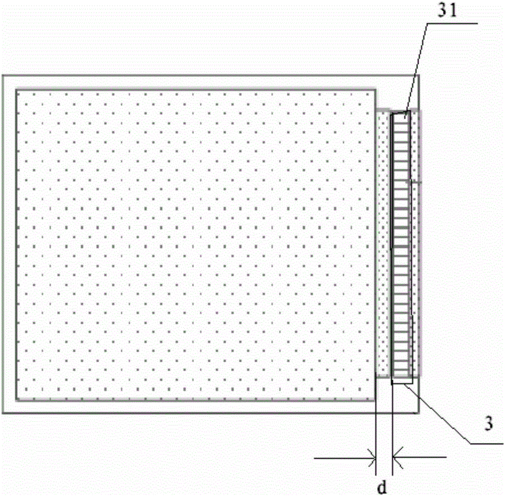
[0045] Such as image 3 As shown, the binding area 3 of the organic light emitting display panel is smaller than the area covered by the connecting terminal 31, and the binding area is a set distance away from the edge of the substrate.

[0046] In the specific implement...


PUM


Abstract

The present invention discloses a packaging method and organic light -emitting display panel of organic glow display panels. Through the packaging method of organic glow display panel provided by the present invention, the narrow frame organic light -emitting display panel can be achieved.question.The packaging method of the organic light -emitting display panel includes a substrate substrate that forms an organic light emitting device and the peripheral binding area to form a water -resistant oxygen layer covering the entire substrate substrate, and the water resistance on the substrate substrateEstor the oxygen layer, etch on the water blocking layer on the substrate substrate, at least remove the water -resistant oxygen layer on the connected terminal in the binding area, and retain the water resistance on the organic luminous deviceOxygen layer.

Description

technical field [0001] The invention relates to the field of display technology, in particular to a packaging method of an organic light emitting display panel and the organic light emitting display panel. Background technique [0002] In the field of display technology, compared with traditional liquid crystal displays, organic light-emitting display panels have gradually become the mainstream in the display field due to their advantages such as fast response speed, wide color gamut, ultra-thin, and flexibility. [0003] The organic light-emitting display panel is provided with a plurality of organic light-emitting diodes (Organic Light Emitting Diode, OLED) arranged in a matrix and circuits in the peripheral binding area. The cathode of the organic light-emitting diode is made of a more active metal, which is easily absorbed by moisture in the air. and oxygen oxidation. Once the cathode is oxidized, the cathode and the organic layer materials in the OLED will be irreversi...

Claims


Application Information

Patent Timeline
Patent Type & Authority Patents(China)
IPC IPC(8): H01L51/56H01L27/32
CPCH10K59/00H10K50/84H10K50/844H10K2102/00H10K71/00
Inventor 藤野诚治曾庆慧
Owner BOE TECH GRP CO LTD
Why Eureka
Try Eureka