

Silicon wafer eccentric tester
A tester and eccentricity technology, applied in the field of silicon wafer eccentricity tester, can solve the problems of high price, difficult to bear and use by optical device companies, and achieve the effects of low price, convenient measurement method and simple equipment
- Summary
- Abstract
- Description
- Claims
- Application Information
AI Technical Summary
Problems solved by technology
Method used
Image

Examples
Embodiment Construction
[0014] In order to deepen the understanding of the present invention, the present invention will be described in further detail below in conjunction with the accompanying drawings and embodiments, which are only used to explain the present invention and do not limit the protection scope of the present invention.
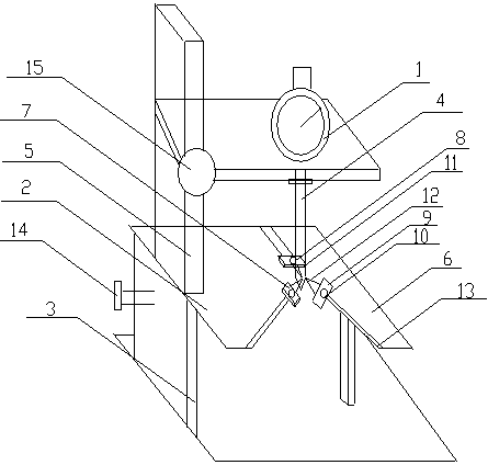
[0015] This embodiment provides a silicon wafer eccentricity tester, comprising a dial indicator 1, a bearing 2, a support base 3, a measuring head 4 and a tester body 5, the bearing 2 is installed on the support base 3, the The tester body 5 is located on one side of the carrier 2, the dial gauge 1 is fixed on the tester body 5, and the side head is installed at the bottom of the dial gauge 1 and vertically Pointing to the center of the carrier 2, the carrier 2 is a three-legged form, including a fixed plate 6, a bracket A7, a bracket B8 and a bracket C9, the fixed plate 6 is a hollowed-out fixed plate 6, and the bracket A7 , bracket B8 and bracket C9 are all instal...
PUM
 Abstract
Description
Claims
Application Information