
Touch control color film base plate, manufacturing method of touch control color film base plate, display panel and display device

A color filter substrate and manufacturing method technology, applied in optics, instruments, electrical digital data processing and other directions, can solve the problems of affecting LCD transmittance, increasing process complexity, and manufacturing processes are not on the same side, so as to reduce process complexity. , The effect of eliminating the inversion process and improving the transmittance

Active Publication Date: 2014-09-17
BEIJING BOE OPTOELECTRONCIS TECH CO LTD
View PDF5 Cites 1 Cited by
  • Summary
  • Abstract
  • Description
  • Claims
  • Application Information

AI Technical Summary

Problems solved by technology

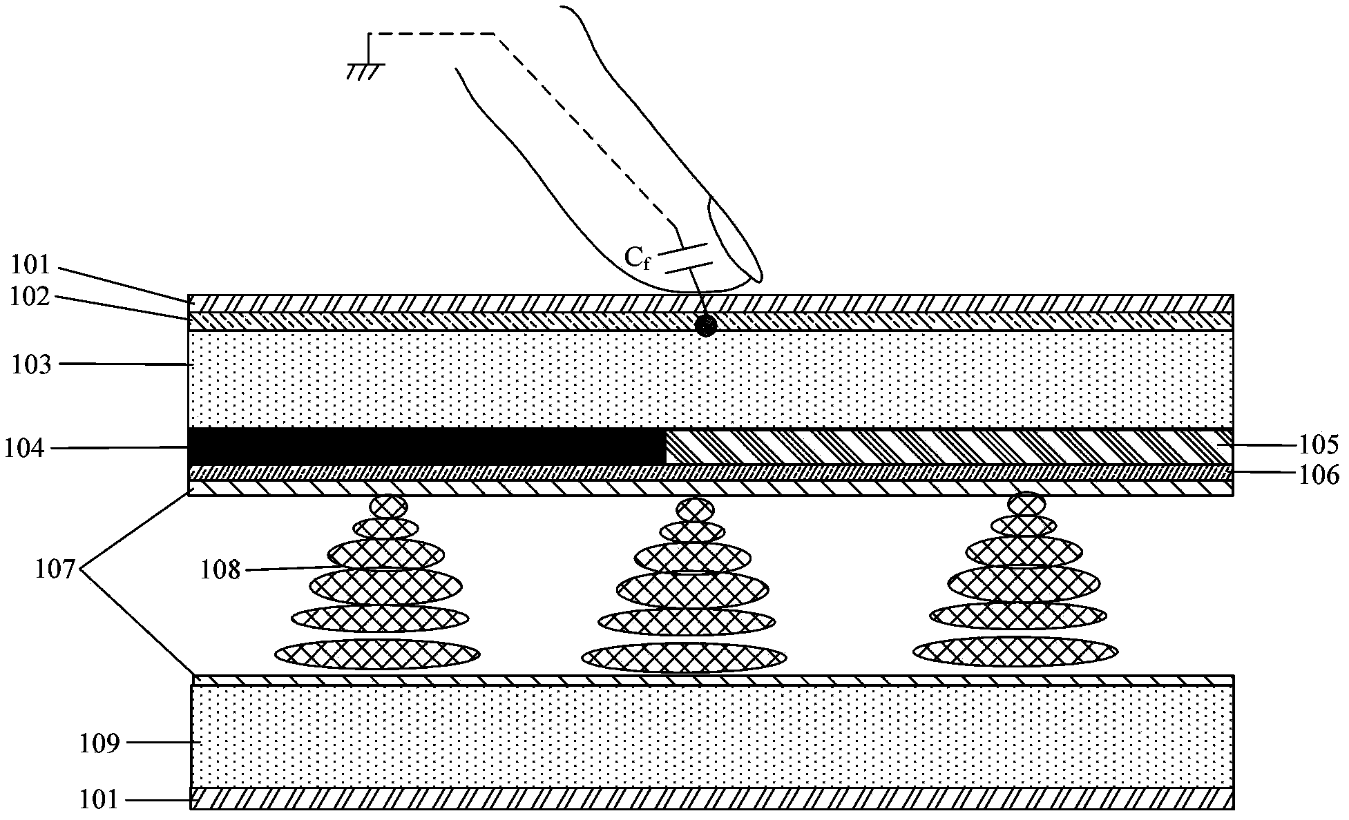
[0004] The existing conventional On-Cell surface capacitive structure is to make a whole conductive layer 102 on the surface of the color filter substrate. The whole conductive layer 102 will affect the transmittance of the LCD; and because the conductive layer 102 is made on the color filter The outer surface of the substrate is not on the same side as the manufacturing process of the color filter substrate, so the substrate flipping process is required, which increases the complexity of the process

Method used


Image

  • Touch control color film base plate, manufacturing method of touch control color film base plate, display panel and display device
  • Touch control color film base plate, manufacturing method of touch control color film base plate, display panel and display device
  • Touch control color film base plate, manufacturing method of touch control color film base plate, display panel and display device

Examples


Embodiment Construction

[0032] The technical solutions of the present invention will be further elaborated below in conjunction with the accompanying drawings and specific embodiments.

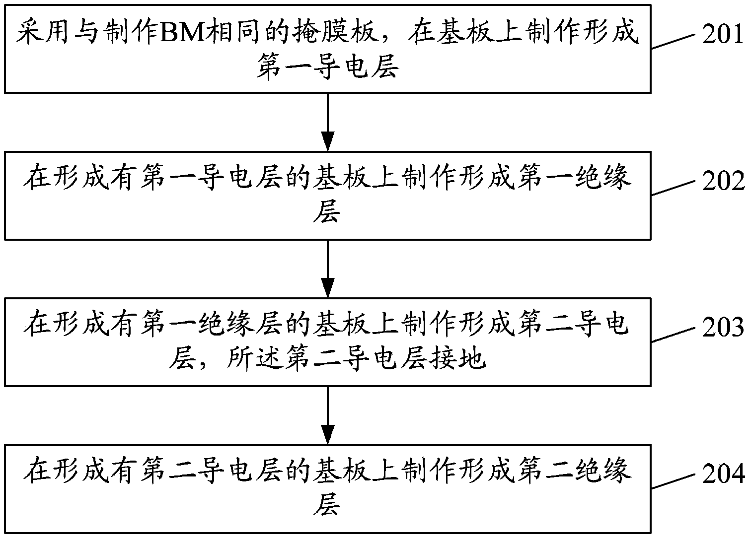
[0033] An embodiment of the present invention provides a method for manufacturing a touch color filter substrate, such as figure 2 As shown, the method mainly includes:

[0034] In step 201, a first conductive layer is formed on a substrate by using the same mask as that used for forming a black matrix (BM).

[0035] The substrate used to make the color filter (CF) substrate may be a glass substrate or a plastic substrate. On the substrate used to fabricate the color filter (CF), the first conductive layer is fabricated and formed using the same mask as that used to fabricate the BM. That is to say, the same mask is used to manufacture the first conductive layer and the BM, so the patterns of the first conductive layer and the BM formed on the touch color filter substrate are the same. The first conductive layer ...


PUM


Abstract

A touch display panel, a manufacturing method thereof, and a display device. The touch display panel comprises a color filter substrate. A first conducting layer (1021) is formed on a base substrate (103) of the color filter substrate, and a first insulating layer (1101) is formed on the first conducting layer (1021). The pattern of the first conducting layer (1021) is identical with the pattern of a black matrix (104) formed on the base substrate (103). The pattern of the first insulating layer (1101) on the display region of the touch display panel is identical with the pattern of the first conducting layer (1021) on the display region.

Description

technical field [0001] The present invention relates to the field of liquid crystal display technology, in particular to a touch color filter substrate and a manufacturing method thereof, a display panel and a display device. Background technique [0002] Liquid crystal displays are currently the mainstream flat panel displays. The realization of the touch function of the LCD panel usually includes two methods: In-Cell and On-Cell. In-Cell refers to the method of embedding the touch panel function into the LCD pixel, and On-Cell refers to the method of embedding the touch panel function into the color film method between substrate and polarizer. [0003] In the prior art, the conventional On-Cell surface capacitive structure for thin film transistor liquid crystal display (TFT-LCD) is as figure 1 As shown, 101 represents a polarizer, 103 represents a substrate (that is, a substrate for a color filter substrate, which may be a glass substrate or a plastic substrate), and a ...

Claims


Application Information

Patent Timeline
Patent Type & Authority Applications(China)
IPC IPC(8): G02F1/1335G02F1/1333G06F3/041
CPCG06F3/041G02F1/1335G02F1/1333G02F1/13338G02F1/133512G06F3/0412G06F3/044G06F2203/04103Y10T29/49105G02F1/133345G02F1/134336
Inventor 刘英明王海生杨盛际刘红娟
Owner BEIJING BOE OPTOELECTRONCIS TECH CO LTD
Learn More