Method for machining PCB through hole

A processing method and technology of via holes, which are applied in the direction of electrical connection formation of printed components, can solve the problems of large reflection of via holes, low bridging strength, and affecting signal transmission performance, so as to improve the impedance of via holes and reduce reflection and loss, the effect of reducing the bottom area

Inactive Publication Date: 2014-10-01
GCI SCI & TECH
View PDF4 Cites 1 Cited by
  • Summary
  • Abstract
  • Description
  • Claims
  • Application Information

AI Technical Summary

Problems solved by technology

The design and processing technology of the existing via hole shielding hole cannot be infinitely approached due to the limitation of PCB drilling accuracy
If the shielding holes are designed to be tangent, the bridging strength will be low, and the remaining signal lines will be easily broken.
At present, there will inevitably be gaps in this type of design, and at the same time, the position of the signal line cannot be drilled for shielding, so that the via hole cannot achieve a good shielding effect, resulting in a large reflection of the via hole during signal transmission, which affects the performance of signal transmission

Method used


Image

  • Method for machining PCB through hole
  • Method for machining PCB through hole
  • Method for machining PCB through hole

Examples


Embodiment Construction

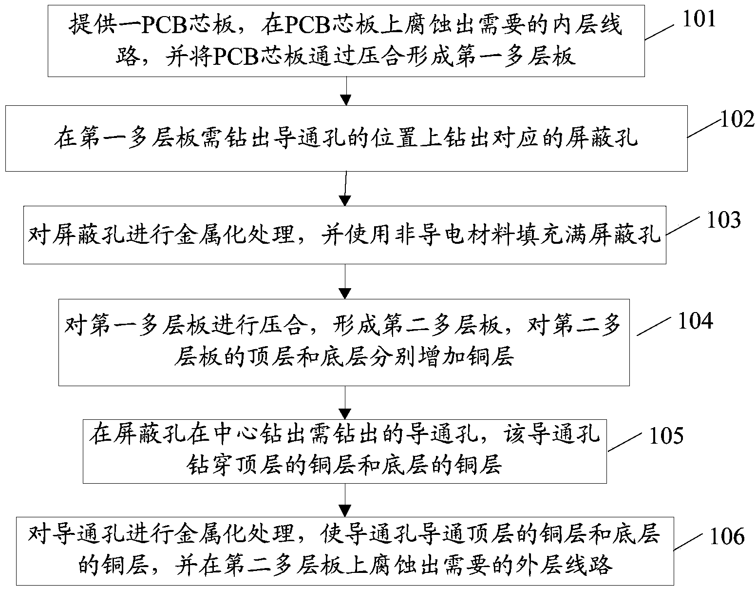
[0026] The following will clearly and completely describe the technical solutions in the embodiments of the present invention with reference to the accompanying drawings in the embodiments of the present invention. Obviously, the described embodiments are only some, not all, embodiments of the present invention. Based on the embodiments of the present invention, all other embodiments obtained by persons of ordinary skill in the art without creative efforts fall within the protection scope of the present invention.

[0027] see figure 1 , is the schematic flow sheet of the processing method of PCB via hole provided by the present invention, and this method is applicable to the production of PCB circuit board, and it mainly comprises the following steps:

[0028] Step 101: Provide a PCB core board, etch the required inner layer circuit on the PCB core board, and press the PCB core board to form a first multi-layer board.

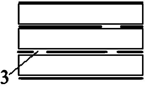
[0029] In this example, if figure 2 As shown, the PCB...


PUM


Abstract

The invention discloses a method for machining a PCB through hole. The method includes the steps that a PCB core board is provided, a needed inner-layer circuit is corroded on the PCB core board, and the PCB core board is pressed to form a first multi-layer board; a corresponding shielding hole is drilled in the position, where the through hole needs to be drilled, on the first multi-layer board, and the diameter of the shielding hole is larger than the diameter of the through hole; metallization processing is carried out on the shielding hole, and the shielding hole is filled with non-conducting materials; the first multi-layer board is pressed again to form a second multi-layer board, and copper layers are additionally arranged on the top layer and the bottom layer of the second multi-layer board respectively; the through hole is drilled in the center of the shielding hole and penetrates through the copper layers on the top layer and the bottom layer in a drilling mode; metallization processing is carried out on the through hole, and a needed outer-layer circuit is corroded on the second multi-layer board. By means of the embodiment, a seamless shielding layer is formed at the position of the through hole, and reflection and losses caused during signal transmission of the PCB through hole are effectively reduced.

Description

technical field [0001] The invention relates to the technical field of circuit board printing, in particular to a method for processing PCB via holes. Background technique [0002] With the rapid development of communication and telecommunication industries, the operating frequency of PCB products is getting higher and higher. The existence of capacitive and inductive reactance in via holes in PCB products leads to more and more serious signal reflection problems at via holes. In order to improve PCB Product transmission performance, reduce loss, via holes in PCB design often reduce the signal reflection of the via holes by adding shielding holes around the via holes, but with the design of adding shielding holes around the via holes, the It is impossible to shield the signal reflection, and the via hole cannot be drilled at the position where the signal line is drawn out. The current shielding hole design and PCB processing technology cannot solve the signal reflection prob...

Claims


Application Information

Patent Timeline
IPC IPC(8): H05K3/42
Inventor 杨泽华任代学李超谋黄德业李金鸿
Owner GCI SCI & TECH
Why Eureka
Try Eureka