Touch substrate and display device

A substrate and touch technology, applied in the direction of instruments, electrical digital data processing, data processing input/output process, etc., can solve the problems of reducing common electrode resistance, uneven distribution of via holes, uneven screen display, etc., to achieve display good effect

Active Publication Date: 2014-10-15
BOE TECH GRP CO LTD +1
View PDF5 Cites 38 Cited by
  • Summary
  • Abstract
  • Description
  • Claims
  • Application Information

AI Technical Summary

Problems solved by technology

[0005] The inventors have found that there are at least the following problems in the prior art: In order to avoid the time delay problem, a plurality of via holes are formed in the common electrode connection bar 100 or the insulating layer corresponding to the common electrode connection bar 100 and the common electrode 300 for common The electrode 300 is connected to the common electrode signal line 1, and the purpose of forming a plurality of via holes is to reduce the resistance of the common electrode, and eac

Method used


Image

  • Touch substrate and display device
  • Touch substrate and display device
  • Touch substrate and display device

Examples


Embodiment 1

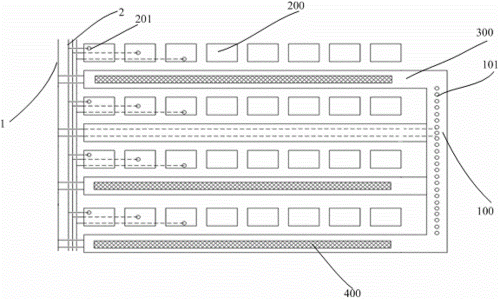
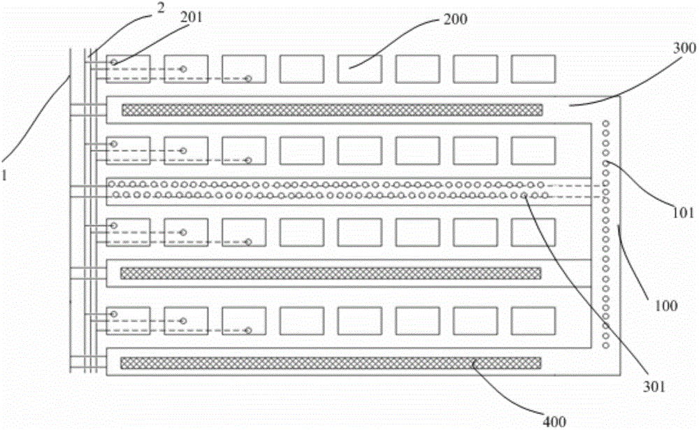
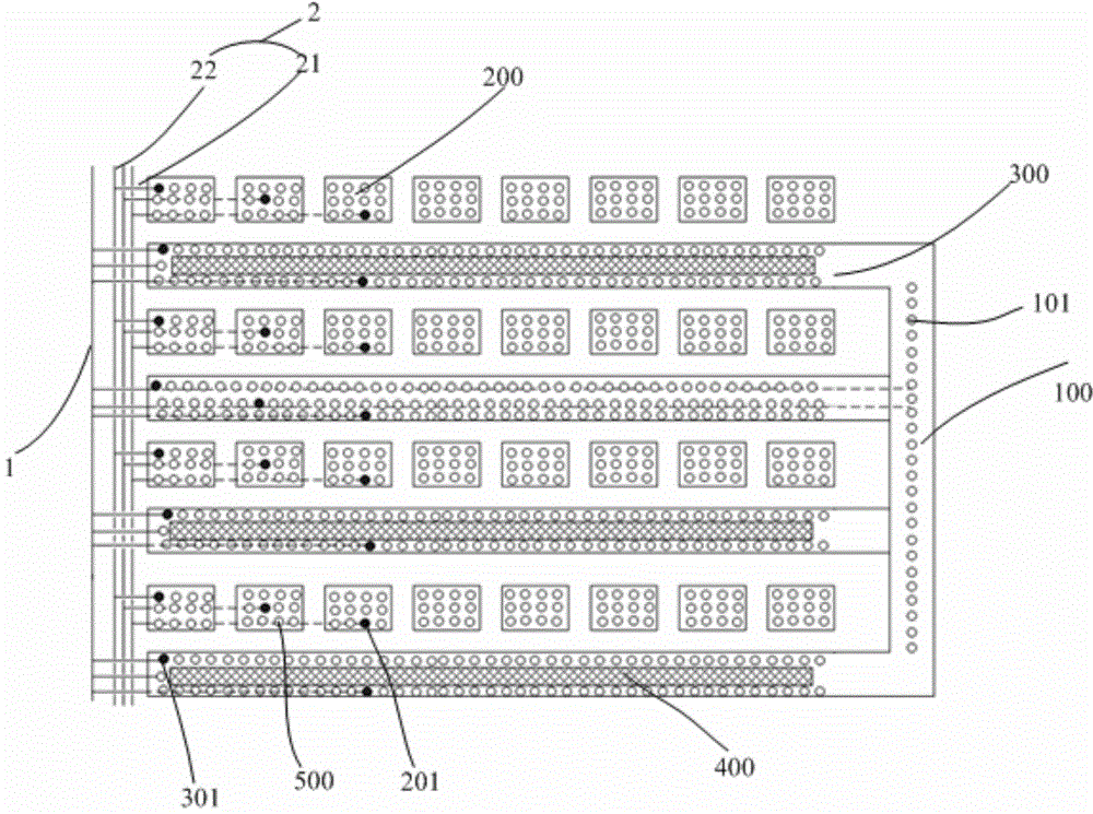
[0027] Such as image 3 As shown, this embodiment provides a touch control substrate, which includes a substrate, an insulating layer disposed on the substrate, a common electrode layer, and a common electrode signal line 1 and a driving electrode signal line 2 disposed on the same layer, wherein the The common electrode 300 layer includes a plurality of driving electrodes, a plurality of common electrodes 300, and a common electrode connection bar 100 connecting each common electrode 300, and each of the driving electrodes includes a plurality of mutually insulated driving sub-electrodes 200 (such as image 3 The driving sub-electrodes in the same column form a driving electrode), the common electrode connection bar 100 is connected to the common electrode signal line 1 through a plurality of first via holes 101 penetrating through the insulating layer, and the driving sub-electrode 200 The driving electrode signal line 2 is connected to the driving electrode signal line 2 th...

Embodiment 2

[0039] This embodiment provides a display device, which includes the touch substrate in Embodiment 1. The display device may be any product or component with a display function such as a mobile phone, a tablet computer, a television, a monitor, a notebook computer, a digital photo frame, a navigator, and the like.

[0040] The display device of this embodiment has the touch substrate in Embodiment 1, so its display effect is better.

[0041] Certainly, the display device of this embodiment may also include other conventional structures, such as a power supply unit, a display driving unit, and the like.


PUM


Abstract

The invention provides a touch substrate and a display device, belongs to the technical field of display, and solves the problem that the display is nonuniform as through holes are not uniformly distributed in the existing touch substrate. The touch substrate at least comprises a base, an insulation layer, a common electrode layer, a common electrode signal wire and a drive electrode signal wire; the insulation layer and the common electrode layer are arranged on the base; the common electrode signal wire and the drive electrode signal wire are arranged on the same layer; the common electrode layer comprises drive electrodes and common electrodes which are arranged in a crossed and insulative way and a common electrode connecting bar which is used for connecting all common electrodes; each drive electrode comprises a plurality of drive sub-electrodes which are mutually insulated; the common electrode connecting bar is connected with the common electrode signal wire by a plurality of first through holes which penetrate through the insulation layer; the drive sub-electrodes are connected with the drive electrode signal wire by a plurality of second through holes which penetrate through the first insulation layer; semi-holes which do not completely penetrate through the insulation layer are formed in the positions, corresponding to the common electrodes and/or the drive sub-electrodes, of the insulation layer.

Description

technical field [0001] The invention belongs to the field of display technology, and in particular relates to a touch substrate and a display device. Background technique [0002] There are many sensing methods of touch screens, such as optical, microwave, resistive, capacitive and so on. Among them, capacitive sensing is the most widely used. Capacitive sensing includes self-capacitance sensing and mutual capacitance sensing. Compared with self-capacitance sensing, mutual capacitance sensing has the advantages of strong anti-interference ability, high sensitivity, multi-touch and recognition capabilities, so mutual capacitance sensing has become the current Mainstream touch screen sensing method. [0003] At present, there are generally two types of mutual capacitance sensing touch screens: in-cell (In Cell) touch screens and non-embedded touch screens. Embedded touch screen means that the sensing electrodes and driving electrodes of the touch screen are arranged inside ...

Claims


Application Information

Patent Timeline
IPC IPC(8): G06F3/044
CPCG06F3/0412G06F3/04164G06F3/0443G06F2203/04111G06F3/0446
Inventor 刘英明董学王海生丁小梁杨盛际赵卫杰邓立广
Owner BOE TECH GRP CO LTD
Why Eureka
Try Eureka