Display panel and manufacturing method thereof

A technology for display panels and manufacturing methods, applied in the fields of nonlinear optics, instruments, optics, etc., which can solve the problems of display panel display panels being white at the periphery of the display panel, unable to prepare ultra-narrow bezel display screens, abnormal display and other problems, Achieve the effect of saving production time, saving wiring space and reducing stirring

Active Publication Date: 2014-10-29
BEIJING BOE OPTOELECTRONCIS TECH CO LTD
View PDF5 Cites 7 Cited by
  • Summary
  • Abstract
  • Description
  • Claims
  • Application Information

AI Technical Summary

Problems solved by technology

However, since the UV transmittance must be considered when the frame sealant is cured by ultraviolet light (UV), it is necessary to reserve a certain space for the peripheral wiring of the display panel, but the frame sealant itself is wide and cannot be compressed. This leads to the inability to prepare display screens with ultra-narrow borders in the prior art
[0003] At the same time, the use of the existing sealing glue process is also prone to breakage and aggregation during the coating process of the sealing glue, resulting in bubbles (Bubble) in the display panel and uneven height around the display panel (Gap), which makes the display panel Whitening and other adverse phenomena; in the process of box alignment and curing, due to the incomplete curing of the sealant, it will cause liquid crystal pollution and the alignment of the above two substrates when the robot picks and places the color film substrate and the array substrate. Deviation, which can easily cause abnormal display and light leakage and other undesirable phenomena

Method used


Image

  • Display panel and manufacturing method thereof
  • Display panel and manufacturing method thereof
  • Display panel and manufacturing method thereof

Examples


Embodiment Construction

[0036] The implementation manner of the present invention will be described in detail below in conjunction with specific embodiments and accompanying drawings.

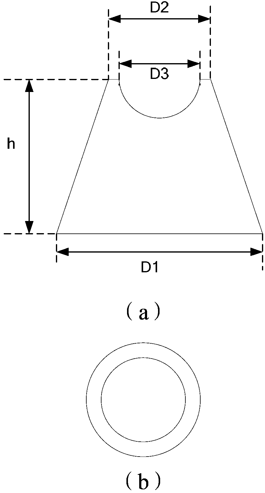
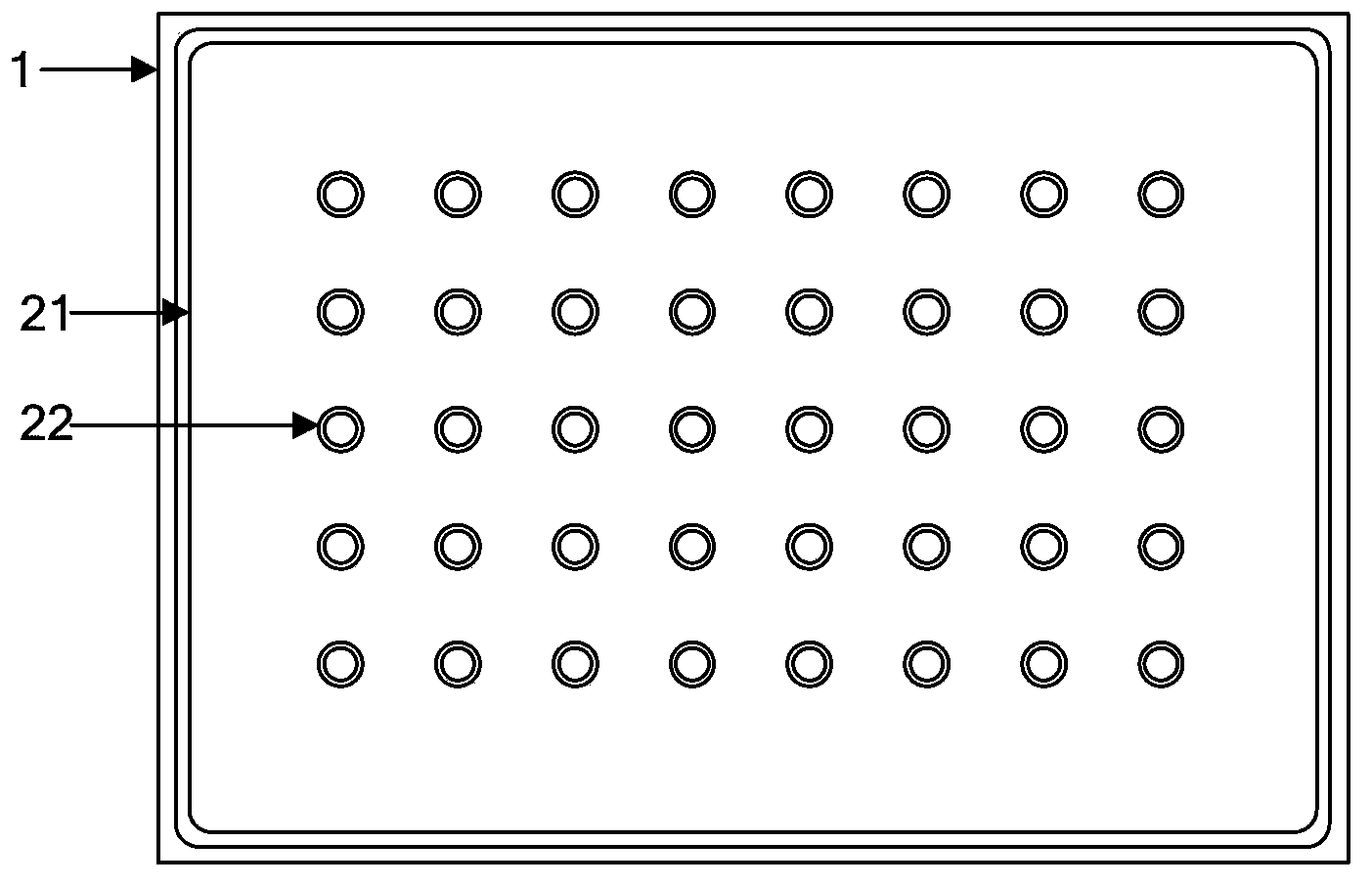
[0037] figure 1 Schematic diagram for the structure of the adsorbed spacer Figure 1 ,in, figure 1 (a) is a cross-sectional view of the adsorbed spacer, figure 1 (b) is a top view of an adsorption spacer; a display panel comprising a first substrate, a second substrate, and an adsorption spacer arranged between the first substrate and the second substrate; wherein, the adsorption spacer An adsorption part is arranged on the spacer, and the first substrate and the second substrate are boxed together through the vacuum adsorption of the adsorption spacer.

[0038] Here, the adsorption part is a groove provided at the top of the adsorption spacer;

[0039] Further, there is at least one groove at the top of the spacer;

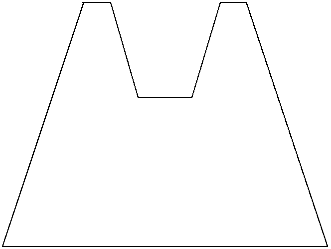
[0040] Further, the shape of the groove is trapezoidal or arc-shaped;

[0041] Further, the ads...


PUM

PropertyMeasurementUnit
widthaaaaaaaaaa
widthaaaaaaaaaa
widthaaaaaaaaaa

Abstract

A display panel, comprising a first substrate (1); a second substrate (3) arranged opposite to the first substrate (1); and an adsorption spacer (2) arranged between the first substrate (1) and the second substrate (3), wherein an adsorption part is arranged on the adsorption spacer (2), and the first substrate (1) and the second substrate (3) are boxed together by means of the vacuum absorption action of the adsorption spacer (2). Also disclosed is a manufacturing method for a display panel.

Description

technical field [0001] The invention relates to the technical field of thin film field effect transistor liquid crystal display (TFT-LCD), in particular to a display panel and a manufacturing method thereof. Background technique [0002] In the existing TFT-LCD process, the frame sealant is usually coated on the periphery of the display panel (Panel) to bond the color filter substrate and the array substrate to form a liquid crystal panel. Here, the frame sealant acts as an adhesive, And the role of supporting the thickness of the box around the display panel. However, since the UV transmittance must be considered when the frame sealant is cured by ultraviolet light (UV), it is necessary to reserve a certain space for the peripheral wiring of the display panel, but the frame sealant itself is wide and cannot be compressed. This leads to the inability to prepare a display screen with an ultra-narrow frame in the prior art. [0003] At the same time, the use of the existing ...

Claims


Application Information

Patent Timeline
Patent Type & Authority Applications(China)
IPC IPC(8): G02F1/1339G02F1/1333
CPCC09K2323/00C09K2323/03C09K2323/057G02F1/13394G02F1/13398
Inventor 蔡佩芝
Owner BEIJING BOE OPTOELECTRONCIS TECH CO LTD
Why Eureka
Try Eureka