A kind of flexible circuit board and preparation method thereof

A flexible circuit board and reinforcing board technology, which is applied in printed circuit manufacturing, printed circuits, printed circuit components, etc., can solve the problems of weak plugging of gold fingers, reduced service life of gold fingers, waste of resources and costs, etc. Achieving the effect of tight and even fit, cost saving and product yield improvement

Active Publication Date: 2019-09-24
EVERDISPLAY OPTRONICS (SHANGHAI) CO LTD
View PDF9 Cites 0 Cited by
  • Summary
  • Abstract
  • Description
  • Claims
  • Application Information

AI Technical Summary

Problems solved by technology

[0003] However, the traditional flexible circuit board has defects in the design of the insertion fingers. The insertion of the gold fingers is not firm, which reduces the service life of the gold fingers and causes waste of resources and costs.

Method used


Image

  • A kind of flexible circuit board and preparation method thereof
  • A kind of flexible circuit board and preparation method thereof
  • A kind of flexible circuit board and preparation method thereof

Examples


Embodiment 1

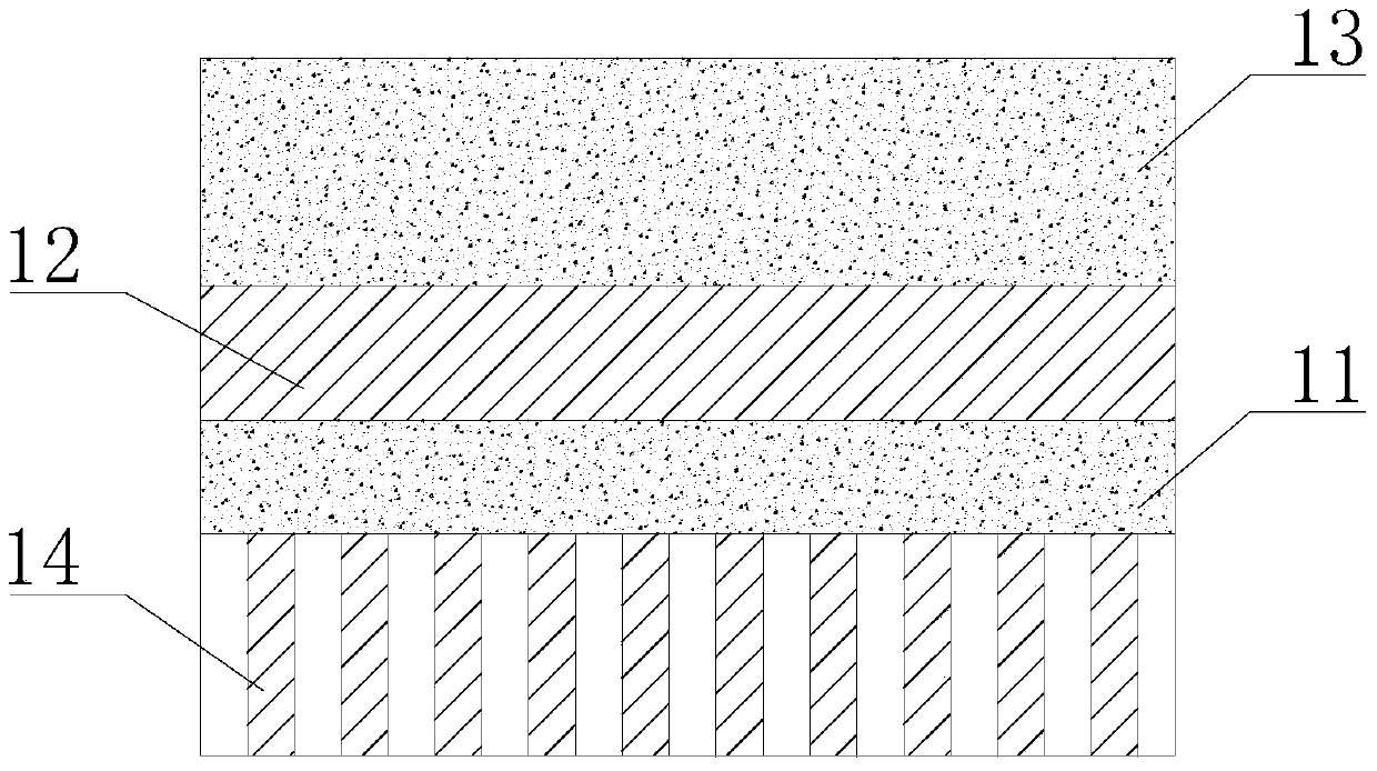
[0016] The flexible circuit board in the embodiment of the present invention, such as figure 1 shown, including:

[0017] The base material 11 has an upper surface and a lower surface opposite to the upper surface; the ground layer 12 is arranged on the upper surface of the base material 11; the reinforcing plate 13 is arranged on the ground layer 12 and covers at least part of the a ground layer; and a conductive pad 14 disposed on the lower surface of the substrate 11 . Wherein, the grounding layer 12 may be made of a metal material, such as copper; the reinforcement board 13 may be a polyimide (PI) reinforcement board; the material of the conductive pad 14 may be copper, nickel or gold or include copper, An alloy material of at least one metal selected from nickel and gold.

[0018] It should be noted that the upper surface and the lower surface of the base material 11 in this embodiment are only an expression method for distinguishing the upper and lower opposite sides o...

Embodiment 2

[0023] The configuration of the structural layers of the flexible circuit board in this embodiment is the same as that in Embodiment 1, and will not be repeated here. The difference is:

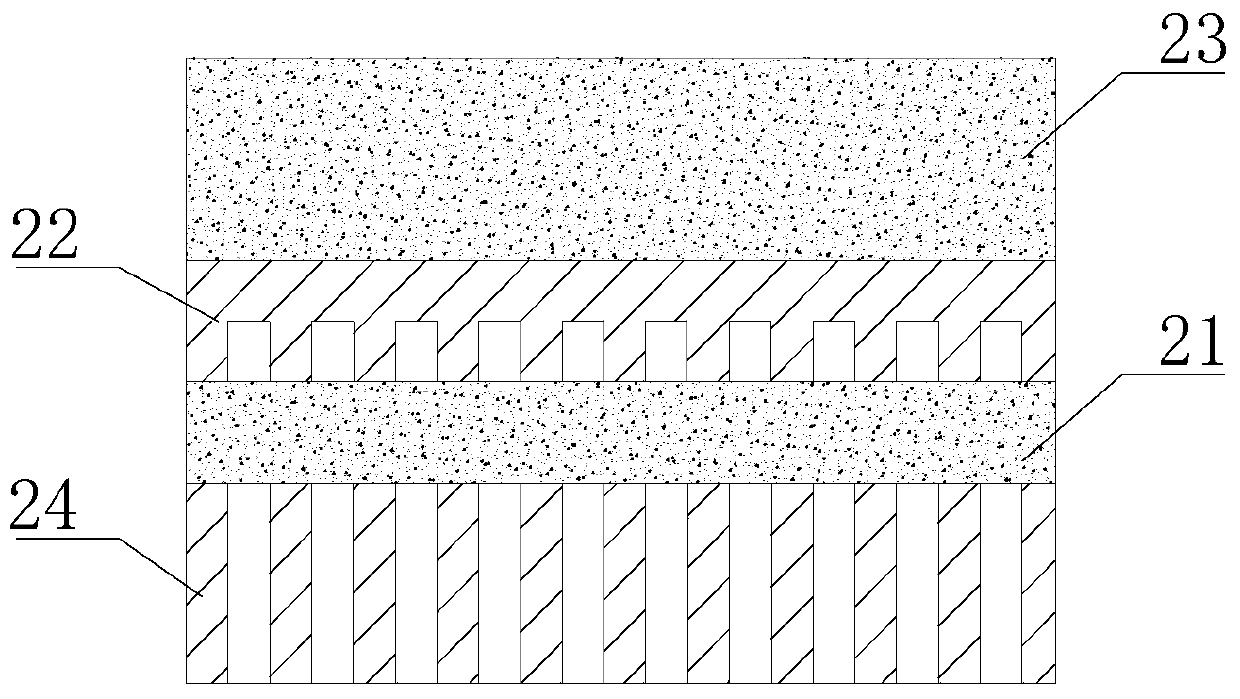
[0024] In Embodiment 1, the part of the ground layer 12 corresponding to the reinforcing plate 13 is a solid layer with a smooth surface, while the ground layer 12 has no part corresponding to the reinforcing plate 13 ( figure 1 and figure 2 (not shown in ), especially the bending part of the ground layer 12 can be set as a grid structure.

[0025] In this example, refer to image 3 , the ground layer 22 can be set as a solid surface (such as solid copper) and the other side of the ground layer 22 that is not in contact with the reinforcement plate 23 (that is, the ground layer 22 is in contact with the substrate 21). One side) is a hollow grid structure.

[0026] In addition, the grounding layer of the flexible circuit board of the present invention also has many variations. As long as...

Embodiment 3

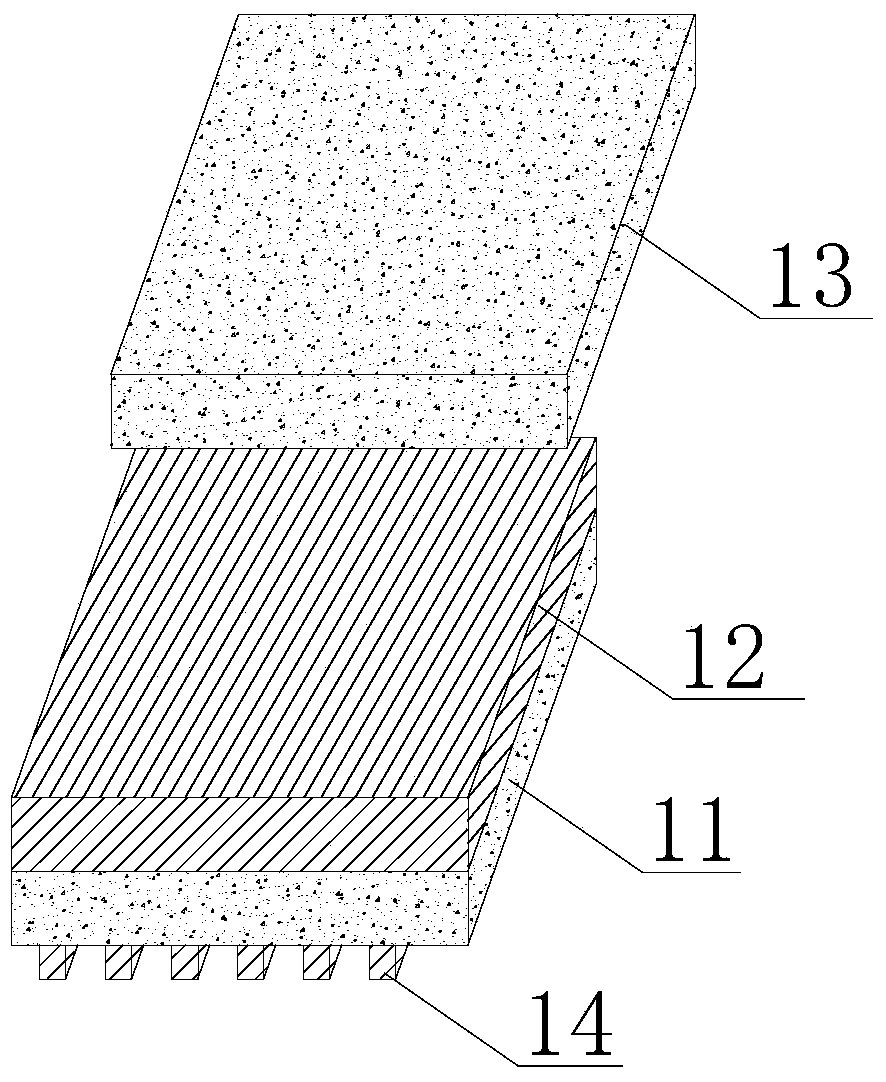
[0028] refer to Figure 4 , this embodiment provides a method for preparing the flexible circuit board in Embodiment 1, including:

[0029] A substrate 11 of insulating material is provided, and the substrate 11 has an upper surface and a lower surface opposite to the upper surface; also as described in Embodiment 1, the upper surface and the lower surface of the substrate 11 here are only the distinguishing base It is a way of expressing the upper and lower opposite sides of the material 11. In practical applications, the subsequent grounding layer 12 and the conductive pad 14 can be prepared on any surface of the base material 11 respectively, as long as the base material 11 is guaranteed to connect the ground layer 12 Just be isolated from the conductive pad 14 .

[0030] Next, a first metal thin film is formed on the upper surface of the substrate 11, and a second metal thin film is formed on the lower surface of the substrate 11; 11 and form a ground layer 12 with a sol...


PUM


Abstract

The invention relates to the field of flexible circuit boards and particularly relates to a flexible circuit board and a manufacturing method thereof. The flexible circuit board comprises a substrate, a grounding layer, a stiffening plate and conductive pads, wherein the substrate has an upper surface and a lower surface opposite to the upper surface; the grounding layer is arranged on the upper surface of the substrate; the stiffening plate is arranged on the grounding layer and at least covers part of the grounding layer; the conductive pads are arranged on the lower surface of the substrate; and the surface, covered by the stiffening plate, of the grounding layer is a solid plane, and the adhesive force between the grounding layer and the stiffening plate is enhanced. The flexible circuit board adopts a solid grounding layer mode on the back surface of the conductive pad, adhesion between the stiffening plate and the grounding layer is tighter and more uniform, the adhesive force of the stiffening plate is enhanced, and the stiffening plate is not likely to fall. The plug-pull times of the conductive pad can also be increased, the cost is saved, and the product yield is improved.

Description

technical field [0001] The invention relates to the field of flexible circuit boards, in particular to a flexible circuit board and a preparation method thereof. Background technique [0002] Flexible circuit boards, also known as "soft boards", are printed circuits made of flexible insulating substrates. Flexible circuits provide excellent electrical performance, can meet the design needs of smaller and higher density mounting, and also help reduce assembly processes and enhance reliability. The flexible circuit board can be bent, wound, and folded freely, and can withstand millions of dynamic bendings without damaging the wires. It can be arranged arbitrarily according to the requirements of the space layout, and can be moved and stretched arbitrarily in the three-dimensional space, so as to achieve the assembly of components and wires. Integration of connections; flexible circuit boards can greatly reduce the volume and weight of electronic products, and are suitable for...

Claims


Application Information

Patent Timeline
Patent Type & Authority Patents(China)
IPC IPC(8): H05K1/09H05K3/02
Inventor 陈虹红
Owner EVERDISPLAY OPTRONICS (SHANGHAI) CO LTD
Why Eureka
Try Eureka