LED packaging structure and method, display device and illuminating device

A technology of LED packaging and LED chips, which is applied in the direction of electrical components, electric solid devices, circuits, etc., can solve the problems of small viewing angle, poor firefly of liquid crystal display devices, and difficult realization, etc., to expand the irradiation range, improve the irradiation effect, and the viewing angle Enhanced effect

Inactive Publication Date: 2014-11-05
BOE OPTICAL SCI & TECH +1
View PDF7 Cites 3 Cited by
  • Summary
  • Abstract
  • Description
  • Claims
  • Application Information

AI Technical Summary

Problems solved by technology

[0004] The existing LED packaging structure has the problem of small viewing angle, such as figure 1 As shown, the viewing angle of the existing LED packaging structure is about 120 degrees, so that the irradiation range and irradiation effect of the LED packaging structure are limited, so when the LED packaging structure is used as the backlight source of the liquid crystal display device, it is very easy to cause the liquid crystal display device bad firefly
[0005] The existing technology generally improves the viewing angle of the LED packaging structure by improving the formula of the phosphor or improving the material of the bracket, but the research and development of these methods is difficult, the research and development cost is high, and it is not easy to realize

Method used


Image

  • LED packaging structure and method, display device and illuminating device
  • LED packaging structure and method, display device and illuminating device
  • LED packaging structure and method, display device and illuminating device

Examples


Embodiment 1

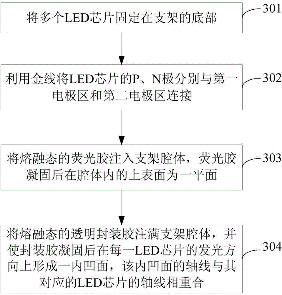
[0091] Such as image 3 As shown, the LED packaging method of this embodiment specifically includes:

[0092] Step 301: fixing multiple LED chips on the bottom of the bracket;

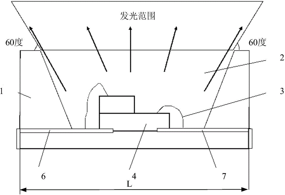
[0093] Such as Figure 4 As shown, the stent 1 has a cavity, and the bottom of the cavity is a metal layer, and the metal layer includes a first electrode area 6 and a second electrode area 7 . Specifically, the LED chip 4 can be fixed on the metal layer by using a die-bonding glue, and the die-bonding glue can be epoxy resin or silica gel. It should be noted that Figure 4 Only the situation of one LED chip 4 is drawn in the figure.

[0094] Step 302: Connect the P and N poles of the LED chip to the first electrode area and the second electrode area respectively with gold wires;

[0095] The P and N poles of the plurality of LED chips 4 are respectively connected to the first electrode region 6 and the second electrode region 7 of the metal layer by gold wires 3 .

[0096] Step 303: inject molten...

Embodiment 2

[0102] Such as Image 6 As shown, the LED packaging method of this embodiment specifically includes:

[0103] Step 501: fixing multiple LED chips on the bottom of the bracket;

[0104] Such as Figure 7 As shown, the stent 1 has a cavity, and the bottom of the cavity is a metal layer, and the metal layer includes a first electrode area 6 and a second electrode area 7 . Specifically, the LED chip 4 can be fixed on the metal layer by using a die-bonding glue, and the die-bonding glue can be epoxy resin or silica gel. It should be noted that Figure 7 Only the situation of one LED chip 4 is drawn in the figure.

[0105] Step 502: Connect the P and N poles of the LED chip to the first electrode area and the second electrode area respectively with gold wires;

[0106] The P and N poles of the plurality of LED chips 4 are respectively connected to the first electrode region 6 and the second electrode region 7 of the metal layer by gold wires 3 .

[0107] Step 503: inject molten...


PUM


Abstract

The invention provides an LED packaging structure and method, a display device and an illuminating device, which belong to the field of photoelectric technology. The LED comprises a bracket with a cavity and at least one LED chip arranged in the cavity, wherein after the cavity is filled with fluorescent glue, at least one concave mirror structure is formed at the light-emitting side of the LED chip. The invention provides an LED packaging structure with wide-viewing angle and an LED packaging method, a display device and an illuminating device. The illuminating range of an LED is enlarged at lower cost and the illuminating effect of the LED is improved.

Description

technical field [0001] The invention relates to the field of optoelectronic technology, in particular to an LED packaging structure and packaging method, a display device, and a lighting device. Background technique [0002] With the development of LED (light emitting diode, light emitting diode) technology, LED has been widely used in more and more technical fields due to its superior performance. For example, various existing display devices use LEDs as light sources, specifically, LEDs are used as backlight sources for liquid crystal televisions. [0003] figure 1 Shown is the existing LED packaging structure, including a bracket 1 with a cavity, the bottom of the cavity is provided with a metal layer, the metal layer includes a first electrode area 6 and a second electrode area 7, on the metal layer There is at least one LED chip 4, the P and N poles of the LED chip 4 are respectively connected to the first electrode area 6 and the second electrode area 7 of the metal ...

Claims


Application Information

Patent Timeline
Patent Type & Authority Applications(China)
IPC IPC(8): H01L33/58
CPCH01L33/483H01L33/54H01L33/58H01L2933/005H01L2933/0058H01L25/0753H01L33/505H01L33/508H01L2224/45144H01L2224/48091H01L2224/49107H01L2924/181H01L2933/0033H01L2933/0041H01L2924/00012H01L2924/00014H01L2924/00
Inventor 王涛
Owner BOE OPTICAL SCI & TECH
Why Eureka
Try Eureka