Voltage comparator
A voltage comparator and power supply technology, applied in the electronic field, can solve the problems of large circuit power consumption, reduced circuit reliability, large actual circuit power consumption, etc., and achieve the effect of low static power consumption and few power consumption branches
- Summary
- Abstract
- Description
- Claims
- Application Information
AI Technical Summary
Problems solved by technology
Method used
Image

Examples
Example Embodiment
[0030] Embodiment one
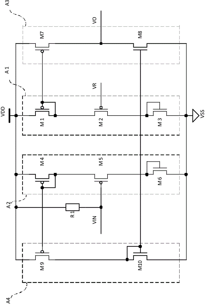
[0031] like figure 2 As shown, the present invention proposes a voltage comparator, including a first branch A1, a second branch A2 and a third branch A3, and the first branch includes a first transistor M1, a second transistor M2 and a third transistor M3 , the source of the first transistor M1 is connected to the power supply VDD, the gate is connected to the drain, and the drain is connected to the drain of the second transistor M2. The gate of the second transistor M2 is connected to the first input terminal VR, and the source is connected to the drain of the third transistor M3. The source of the third transistor M3 is grounded to VSS, and the drain is connected to the gate. The first branch A1 has a self-bias function, and does not need an external input bias signal to control its current magnitude. The current in the A1 branch is proportional to VR, because the higher the VR is, the smaller the on-resistance of the second transistor M2 is, an...
Example Embodiment
[0040] Embodiment two
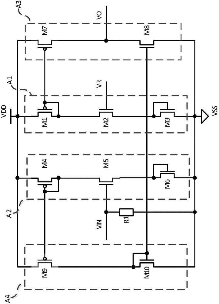
[0041] like image 3 As shown, the difference between the voltage comparator in this embodiment and the first embodiment is that one end of the first resistor R1 is connected to the second input terminal VIN, and the other end is connected to the power supply VDD. In this embodiment, the first transistor M1 , the second transistor M2 , the fourth transistor M4 , the fifth transistor M5 and the seventh transistor M7 are PMOS, and the third transistor M3 , the sixth transistor M6 and the eighth transistor M8 are NMOS.
Example Embodiment
[0042] Embodiment three
[0043] like Figure 4 As shown, a voltage comparator disclosed in this embodiment includes a first branch A1, a second branch A2 and a third branch A3, and the first branch A1 includes a first transistor M1, a second transistor M2 and a first transistor M1. Three transistors M3, the source of the first transistor M1 is connected to the power supply VDD, the gate is connected to the drain, and the drain is connected to the drain of the second transistor M2. The gate of the second transistor M2 is connected to the first input terminal VR, and the source is connected to the drain of the third transistor M3. The source of the third transistor M3 is grounded to VSS, and the drain is connected to its gate.
[0044] The second branch A2 includes a fourth transistor M4, a fifth transistor M5 and a sixth transistor M6. The source of the fourth transistor M4 is connected to the power supply VDD, the gate is connected to the drain, and the drain is connected t...
PUM
 Abstract
Description
Claims
Application Information
 - R&D Engineer
- R&D Manager
- IP Professional
- Industry Leading Data Capabilities
- Powerful AI technology
- Patent DNA Extraction
Browse by: Latest US Patents, China's latest patents, Technical Efficacy Thesaurus, Application Domain, Technology Topic.
© 2024 PatSnap. All rights reserved.Legal|Privacy policy|Modern Slavery Act Transparency Statement|Sitemap