
An optical coupling microstructure device

A technology for coupling devices and microstructures, which is applied to instruments, electrical digital data processing, and input/output processes of data processing. cost, the effect of improving the touch effect

Active Publication Date: 2017-06-30
TSD ELECTRONICS TECH
View PDF3 Cites 0 Cited by
  • Summary
  • Abstract
  • Description
  • Claims
  • Application Information

AI Technical Summary

Problems solved by technology

[0004] For this reason, the technical problem to be solved by the present invention is that the coupling efficiency of the method used for optical path coupling of the touch screen in the prior art is low, and it is difficult to realize a parallel light source with a large radiation solid angle with a small size and high device cost. coupled microstructure device

Method used

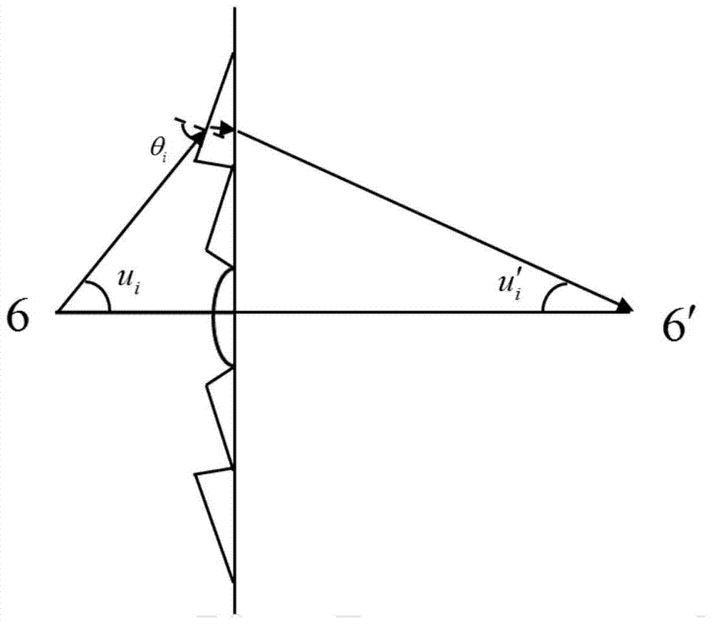
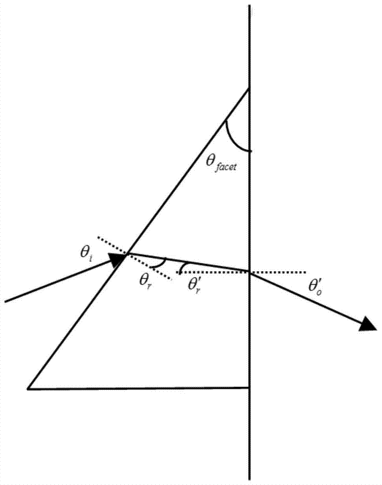

Image

  • An optical coupling microstructure device
  • An optical coupling microstructure device
  • An optical coupling microstructure device

Examples


Embodiment 1

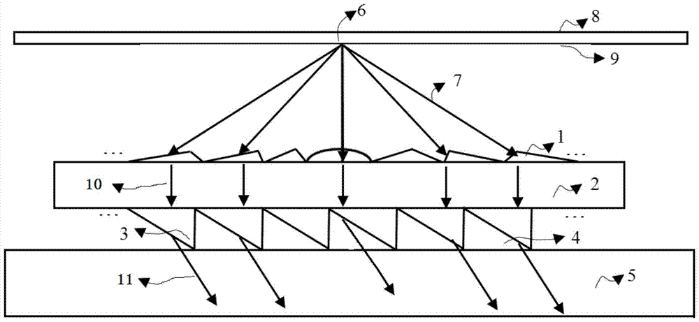
[0038] This embodiment provides an optical coupling microstructure device, such as figure 1 shown, including:

[0039] a first base layer 2;

[0040] Fresnel microstructure layer 1, which is arranged on the first surface of the first base layer, for refracting the light 7 incident on the Fresnel microstructure layer to be perpendicular to the direction of the first base layer the first parallel light 10; and

[0041] Refracting optical path microstructure layer 3, which is arranged on the second surface of the first base layer opposite to the first surface, for refracting the first parallel light to form a certain angle with the device 5 to be coupled The second parallel light 11.

[0042] The signal light source 6 is arranged on the diffuse reflection surface 9 of the PCB 8 and directly above the center of the Fresnel microstructure layer. The signal light source can be an infrared LED with a lower cost. Between the PCB board and the Fresnel microstructure layer is an air...


PUM


Abstract

The invention provides an optical coupling micro-structure device which comprises a first substrate layer, a Fresnel micro-structure layer and a light path turning micro-structure layer. The Fresnel micro-structure layer is arranged on the first surface of the first substrate layer and used for refracting light entering the Fresnel micro-structure layer into first parallel light perpendicular to the first substrate layer. The light path turning micro-structure layer is arranged on the second surface, opposite to the first surface, of the first substrate layer and used for refracting the first parallel light into second parallel light, wherein certain angles are formed between the second parallel light and the first substrate layer. A small-size parallel light source with a large radiation solid angle can be omitted, and cost can be saved; the incident angle of the second parallel light and a device to be coupled can be controlled, then the specific gravity of target light, namely the light subject to total internal reflection is controlled, the coupling efficiency of a signal light source is further improved, and the touch effect is improved; the whole optical coupling micro-structure device has the advantages of being light and thin.

Description

technical field [0001] The invention relates to the technical field of infrared touch, in particular to an optical coupling microstructure device. Background technique [0002] A touch panel is an input device for operating equipment by directly touching a screen such as a liquid crystal display with a finger or a dedicated pen. Touch panels are generally used in ATMs at financial institutions, ticket vending machines at train stations, and portable game machines. Touch screen technologies include: resistive touch screen technology, capacitive touch screen technology, acoustic touch screen technology, infrared touch screen technology and optical touch screen technology. Infrared touch screen technology and optical touch screen technology are simple in principle, easy to generate, low in cost, and suitable for medium and large-sized product applications, but the touch accuracy is low. In the prior art, the technology of frustrated total internal reflection is used to realize...

Claims


Application Information

Patent Timeline
Patent Type & Authority Patents(China)
IPC IPC(8): G06F3/042
Inventor 陈策王志旭徐响林张新泉
Owner TSD ELECTRONICS TECH
Learn More