Liquid crystal display panel and method for manufacturing same

A technology for liquid crystal display panels and manufacturing methods, applied in nonlinear optics, instruments, optics, etc., can solve the problems of large dislocation distance, affecting display effect, and low pixel penetration rate, so as to eliminate dark areas and improve liquid crystal display. Efficiency, the effect of ensuring pixel penetration

Active Publication Date: 2014-12-10
TCL CHINA STAR OPTOELECTRONICS TECH CO LTD
View PDF8 Cites 6 Cited by
  • Summary
  • Abstract
  • Description
  • Claims
  • Application Information

AI Technical Summary

Problems solved by technology

The reason for the appearance of the dark area is that the dislocation (Shift) of the upper and lower substrates of the liquid crystal display panel is the most serious here, and the dislocation distance is relatively large, which makes the black matrix (Black Matrix, BM) additional shading the most, resulting in the liquid crystal display panel here. The pixel penetration rate of the area is lower than that of other areas, which seriously affects the display effect

Method used


Image

  • Liquid crystal display panel and method for manufacturing same
  • Liquid crystal display panel and method for manufacturing same
  • Liquid crystal display panel and method for manufacturing same

Examples


Embodiment Construction

[0021] The technical solutions in the embodiments of the present invention will be clearly and completely described below in conjunction with the accompanying drawings in the embodiments of the present invention. Obviously, the embodiments described below are only part of the embodiments of the present invention, not all of them. Example. Based on the embodiments of the present invention, all other embodiments obtained by persons of ordinary skill in the art without creative efforts fall within the protection scope of the present invention.

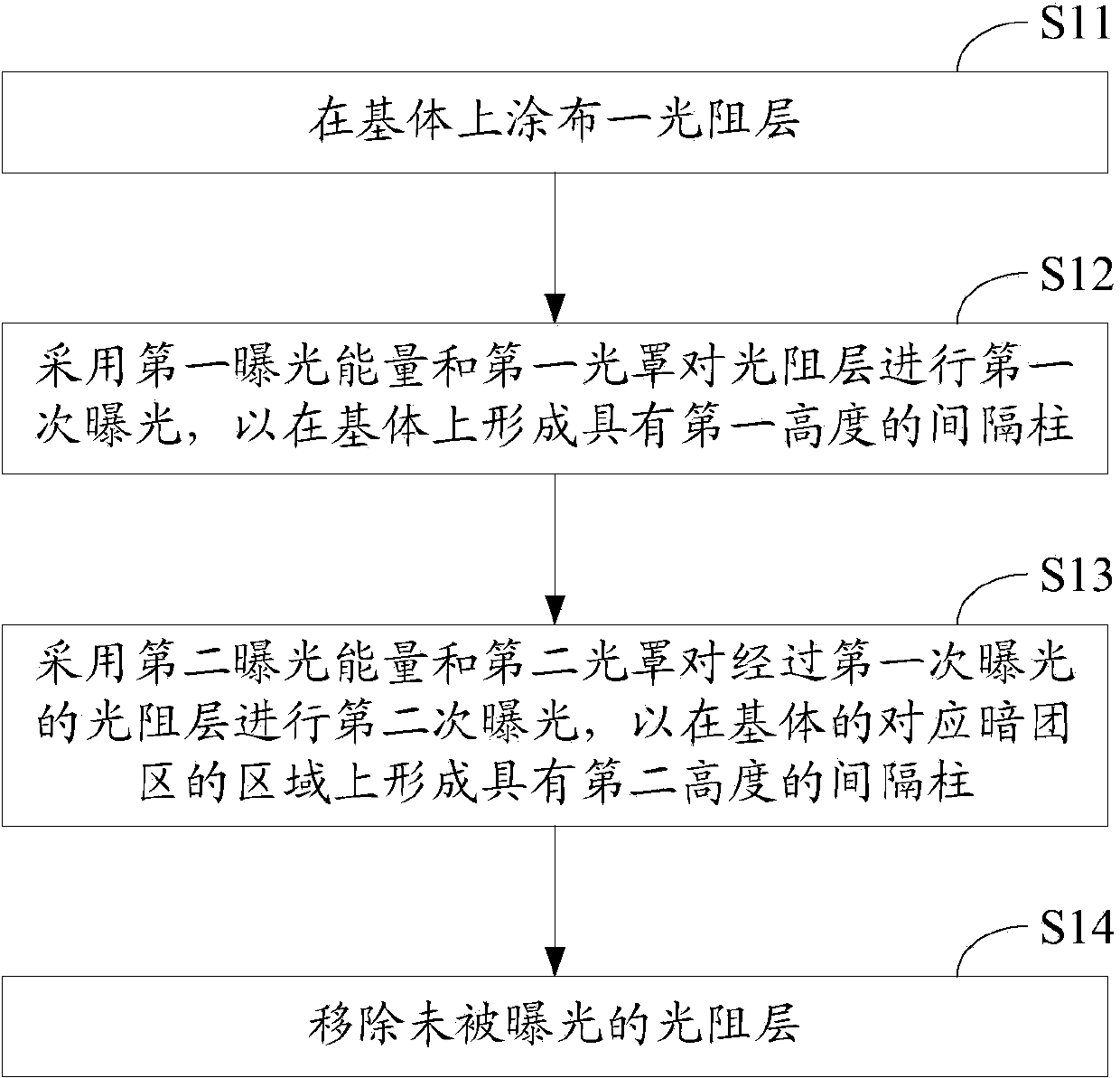
[0022] figure 1 It is a flowchart of the manufacturing method of the liquid crystal display panel of the preferred embodiment of the present invention. Such as figure 1 As shown, the manufacturing method of the liquid crystal display panel of this embodiment includes the following steps:

[0023] Step S11: coating a photoresist layer on the substrate.

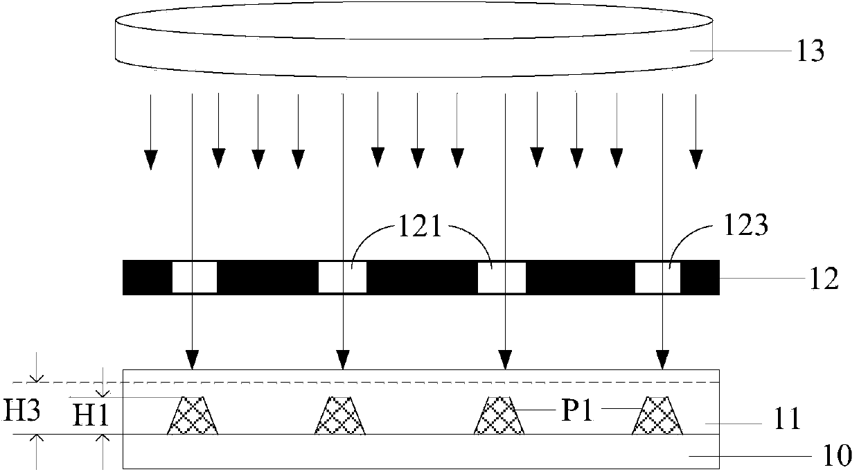
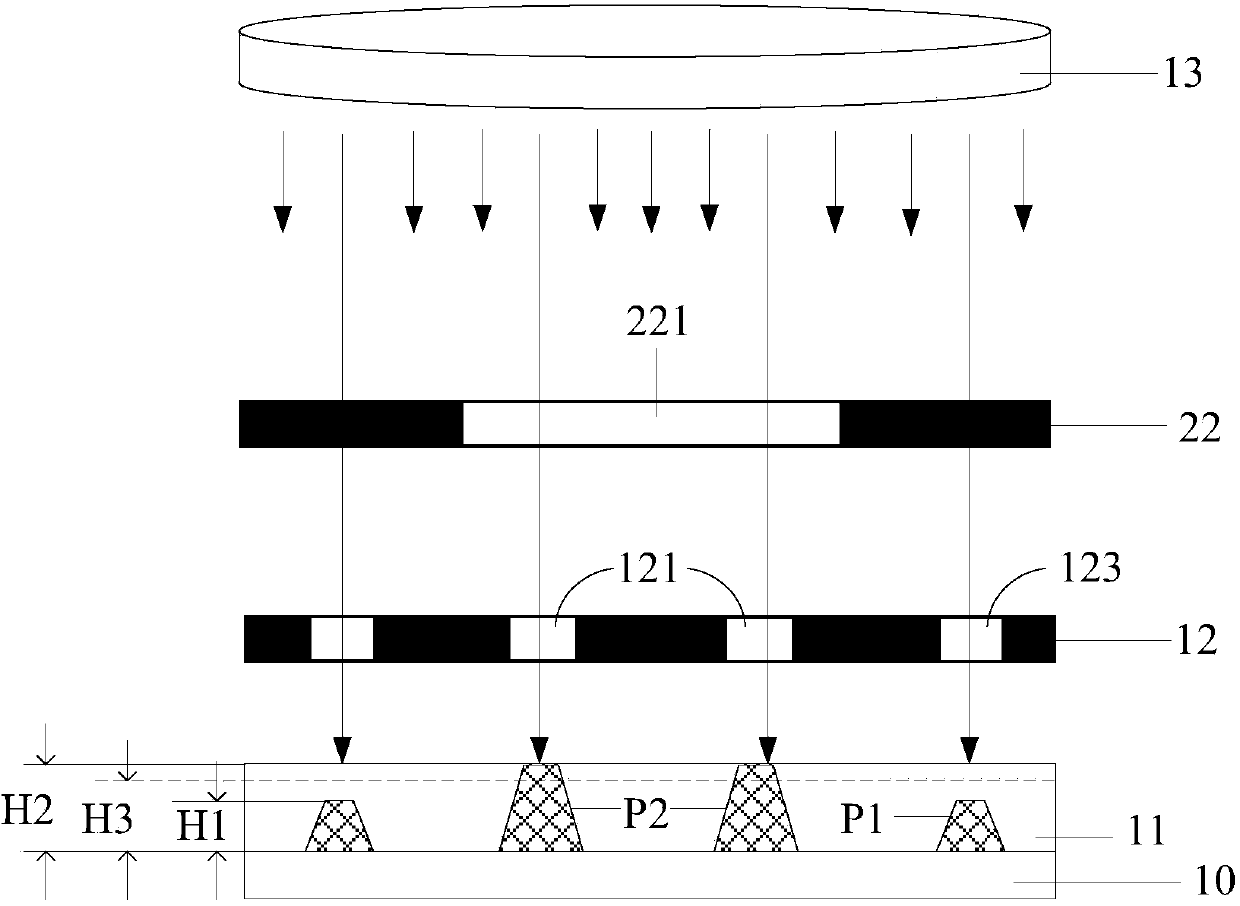
[0024] Such as figure 2 As shown, the substrate 10 corresponds to a color filter...


PUM


Abstract

The invention provides a liquid crystal display panel and a method for manufacturing the same. The method for manufacturing the liquid crystal display panel includes coating a photoresistance layer on a matrix; primarily exposing the photoresistance layer by the aid of first exposure energy and a first photomask to form spacing columns with first heights; secondarily exposing the photoresistance layer by the aid of second exposure energy and a second photomask to form spacing columns with second heights; removing unexposed portions of the photoresistance layer. The first photomask is provided with first transmittance zones corresponding to dark cluster zones. The second photomask is provided with second transmittance zones corresponding to dark cluster zones, and the second heights are larger than the first heights. Owing to the mode, the liquid crystal display panel and the method have the advantages that the efficiency of liquid crystal in the dark cluster zones can be enhanced, the penetration rates of pixels in the dark cluster zones can be guaranteed, and accordingly the dark cluster zones of the liquid crystal display panel can be reduced or eliminated.

Description

technical field [0001] The invention relates to the technical field of liquid crystal display, in particular to a liquid crystal display panel and a manufacturing method thereof, so as to reduce or eliminate dark areas generated during curved surface display. Background technique [0002] Currently, liquid crystal display panels, such as TFT-LCD (Thin Film Transistor-Liquid Crystal Display, Thin Film Transistor-Liquid Crystal Display, Thin Film Transistor-Liquid Crystal Display, thin film transistor liquid crystal display) panels, are prone to dark areas at the most serious bending (Bending) of the curved surface, and generally It is located near halfway from the center of the liquid crystal display panel to the left and right edges respectively. The reason for the appearance of the dark area is that the dislocation (Shift) of the upper and lower substrates of the liquid crystal display panel is the most serious here, and the dislocation distance is relatively large, which m...

Claims


Application Information

Patent Timeline
Patent Type & Authority Applications(China)
IPC IPC(8): G02F1/13G02F1/1339
CPCG02F1/13G02F1/1339
Inventor 郑华
Owner TCL CHINA STAR OPTOELECTRONICS TECH CO LTD
Why Eureka
Try Eureka