TFT (Thin Film Transistor) array substrate

一种阵列基板、阵列式的技术,应用在光学、仪器、电气元件等方向,能够解决偶数列子像素充电不足、偶数列子像素亮度不足等问题,达到改善显示缺陷、避免错充显现、整体电阻变小的效果

Active Publication Date: 2015-01-07
TCL CHINA STAR OPTOELECTRONICS TECH CO LTD
View PDF12 Cites 40 Cited by
  • Summary
  • Abstract
  • Description
  • Claims
  • Application Information

AI Technical Summary

Problems solved by technology

When the scan lines G1, G2, G3, G4, etc. are turned on sequentially, the even-numbered sub-pixels connected to both sides of each data line are sequentially driven row by row before the odd-numbered sub-pixels, for example, the sub-pixels P12, P13, P22, and P23 are driven sequentially. In the period of the same polarity of the data signal, the sub-pixels driven later are always charged better than the sub-pixels driven first. In this way, P13 is better charged than P12, and P23 is better charged than P22. After sex reversal, the driving sequence remains unchanged, and the even-numbered sub-pixels are still driven first, and then the odd-numbered sub-pixels are driven; The sub-pixels in the even-numbered columns may be insufficiently charged, so that the brightness of the positions corresponding to the sub-pixels in the even-numbered columns is insufficient, and the defect of vertical bright and dark lines is formed from the perspective of the overall display effect.

Method used


Image

  • TFT (Thin Film Transistor) array substrate
  • TFT (Thin Film Transistor) array substrate
  • TFT (Thin Film Transistor) array substrate

Examples


Embodiment Construction

[0033] In order to further illustrate the technical means adopted by the present invention and its effects, the following describes in detail in conjunction with preferred embodiments of the present invention and accompanying drawings.

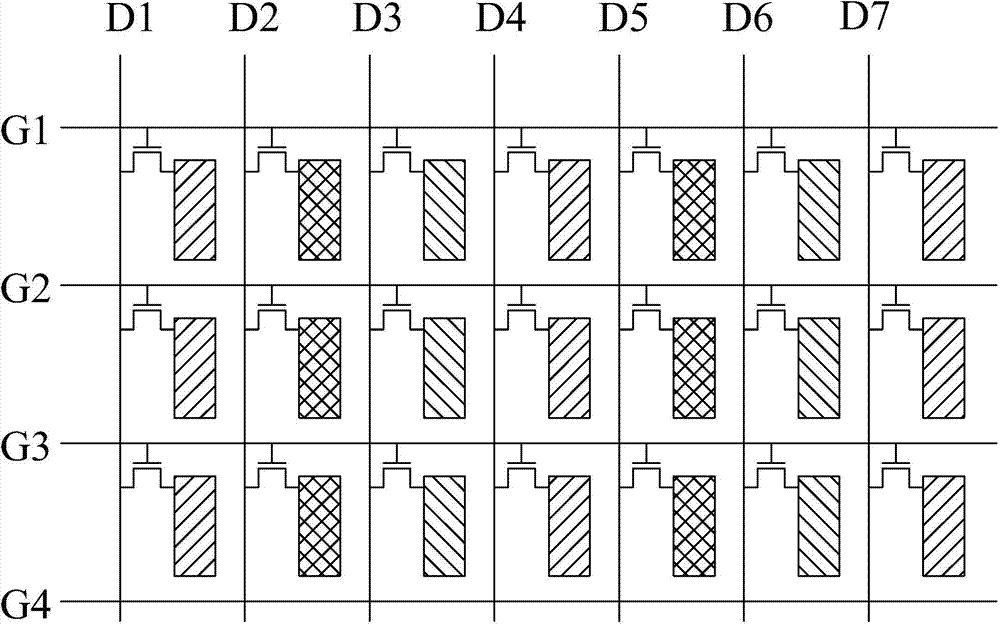
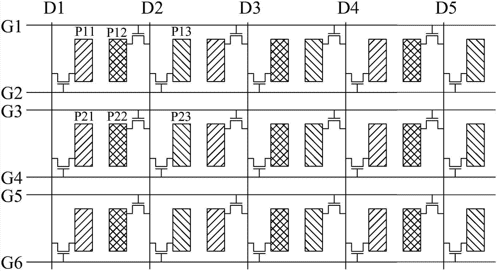
[0034] see Figure 5 , is a schematic diagram of the first embodiment of the TFT array substrate of the present invention. The TFT array substrate includes: a plurality of data lines, such as D1, D2, D3, D4, etc., a plurality of scanning lines, and a plurality of sub-pixels in an array.

[0035] The sub-pixels in the odd-numbered columns and the sub-pixels in the even-numbered columns in each row of sub-pixels are laterally staggered on the plane.

[0036] Each data line is electrically connected to two sub-pixels on the left and right sides of the data line in each row of sub-pixels through TFTs, and provides data signals for the two sub-pixels.

[0037] Corresponding to each row of sub-pixels, two scanning lines are respectively located on...


PUM


Abstract

The invention provides a TFT (Thin Film Transistor) array substrate. The arrangement mode of sub-pixels is changed to enable the uneven brightness of sub-pixels on the space to be arranged in a staggered mode in the same frame image display cycle and accordingly the display defects of vertical bright and dark lines are overcome. The integral resistance of data lines can be reduced, the resistance capacity delay is reduced, and accordingly the wrong charging display of the tail ends of scanning lines or the data lines is avoided.

Description

technical field [0001] The present invention relates to the field of display technology, in particular to a TFT array substrate. Background technique [0002] In the field of display technology, flat-panel displays such as Liquid Crystal Display (LCD) and Organic Light Emitting Diode (OLED) have gradually replaced CRT displays, and are widely used in LCD TVs, mobile phones, personal digital assistants, digital Cameras, computer or laptop screens, etc. [0003] The display panel is an important part of LCD and OLED. Whether it is an LCD display panel or an OLED display panel, it usually has a thin film transistor (Thin Film Transistor, TFT) array substrate. A plurality of R, G and B sub-pixels arranged in an array, a plurality of scanning lines, and a plurality of data lines are formed on the TFT array substrate. Each sub-pixel receives a scan signal through a corresponding scan line and a data signal through a corresponding data line to display an image. [0004] figure...

Claims


Application Information

Patent Timeline
Patent Type & Authority Applications(China)
IPC IPC(8): G02F1/13G02F1/1362
CPCG02F1/136286G09G3/3614G09G2320/0233G09G3/3659G09G2320/0223H01L27/124G09G3/3266G09G3/3275G09G3/3677G09G3/3688G09G2300/0809G09G2310/0278G02F1/1362
Inventor 陈彩琴许哲豪
Owner TCL CHINA STAR OPTOELECTRONICS TECH CO LTD
Why Eureka
Try Eureka