Light-emitting diode packaging structure and manufacturing method thereof
A technology of light-emitting diodes and packaging structures, which is applied to electrical components, electrical solid devices, circuits, etc., can solve problems such as side light leakage, and achieve the effect of preventing side light leakage
- Summary
- Abstract
- Description
- Claims
- Application Information
AI Technical Summary
Problems solved by technology
Method used
Image

Examples
no. 1 example 〕
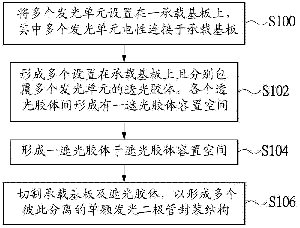
[0030] see Figure 1 to Figure 4 As shown, the first embodiment of the present invention provides a method for manufacturing a light emitting diode (LED) packaging structure Z for preventing side light leakage. Such as figure 1 Shown flow process step, it comprises the following steps:
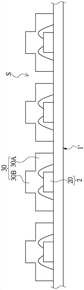
[0031] Step S100: Matching figure 2 As shown, a plurality of light emitting units 2 are disposed on a carrier substrate 1', wherein the plurality of light emitting units 2 are electrically connected to the carrier substrate 1'. For example, each light emitting unit 2 includes at least one light emitting diode chip 20, and the light emitting diode chip 20 can be electrically connected to the carrier substrate 1' through two wires (not labeled);
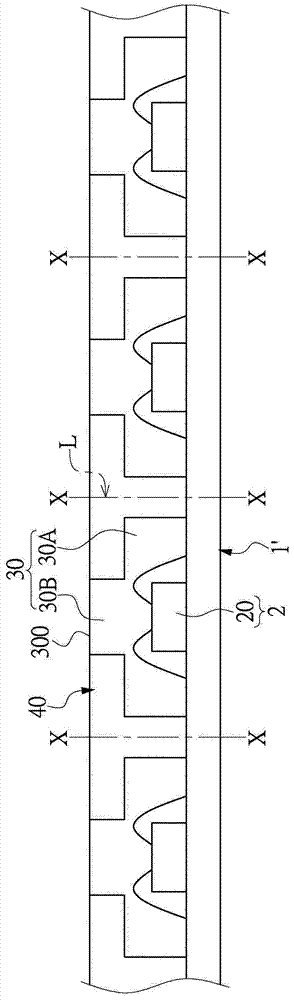
[0032] Step S102: Matching figure 2 As shown, a plurality of light-transmitting colloids 30 are formed on the carrier substrate 1' and respectively cover a plurality of light-emitting units 2, which may be transparent colloids, colloids with fluo...
no. 2 example
[0037] see Figure 5 to Figure 6 As shown, the second embodiment of the present invention provides another manufacturing method of a light emitting diode (LED) packaging structure Z for preventing side light leakage. Wherein, step S200, steps S206-S208 of this embodiment are the same as step S100, steps S104-S106 of the above-mentioned embodiment respectively, so no more details are given here. The biggest difference between this embodiment and the above-mentioned embodiment is the following steps:
[0038] Step S202: cooperation Image 6 As shown, a light-transmitting glue 30 disposed on the carrier substrate 1' and covering a plurality of light-emitting units 2 is formed. Furthermore, the transparent colloid 30 can be a transparent colloid, a colloid with fluorescent particles or a colloid with diffusion particles, and the transparent colloid 30 has an 20 of the first light-transmitting portion 30A and at least one second light-transmitting portion 30B protruding upward f...
no. 3 example
[0041] see Figure 7 As shown, the third embodiment of the present invention can provide a light emitting diode packaging structure Z for preventing side light leakage, which includes: a substrate unit 1 , a light emitting unit 2 , a light transmitting unit 3 and a light shielding unit 4 . Depend on Figure 7 and Figure 4 The comparison shows that the biggest difference between this embodiment and the above-mentioned embodiment is that the light-transmitting unit 3 further includes a plurality of fluorescent particles 31 evenly distributed in the light-transmitting colloid 30 and a plurality of diffusion particles evenly distributed in the light-transmitting colloid 30. Particles 32, wherein a plurality of diffusing particles 32 can be used to increase the light extraction efficiency of the present invention. In other words, the light-transmitting unit 3 can be formed by mixing the light-transmitting colloid 30 , a plurality of fluorescent particles 31 , and a plurality of ...
PUM
 Abstract
Description
Claims
Application Information
 - R&D Engineer
- R&D Manager
- IP Professional
- Industry Leading Data Capabilities
- Powerful AI technology
- Patent DNA Extraction
Browse by: Latest US Patents, China's latest patents, Technical Efficacy Thesaurus, Application Domain, Technology Topic.
© 2024 PatSnap. All rights reserved.Legal|Privacy policy|Modern Slavery Act Transparency Statement|Sitemap