Packaging cover plate, display panel and display device
A technology for encapsulating cover plates and display substrates, which is applied in the direction of semiconductor devices, electrical components, circuits, etc., can solve the problems of electrode disconnection, virtual connection, and easy cracking, and achieve the effect of preventing lateral light leakage
- Summary
- Abstract
- Description
- Claims
- Application Information
AI Technical Summary
Problems solved by technology
Method used
Image

Examples
Embodiment 1
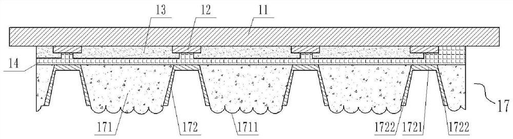
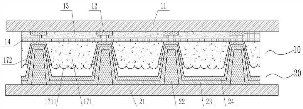
[0057] Such as Figure 2-4 As shown, the packaging cover plate 10 provided in this embodiment includes a cover plate 11, a black matrix 12 and a color filter layer 13 formed on the cover plate 11, and a flat surface covering the black matrix 12 and the color filter layer 13. layer 14, and the first auxiliary electrode unit 17 disposed on the flat layer 14, the color filter layer 13 includes a red color filter, a green color filter and a blue color filter, and the black matrix 12 and the color filter layer 13 are arranged at intervals. Wherein, the first auxiliary electrode unit 17 includes a light guide column 171 and a first auxiliary electrode 172, the light guide column 171 is formed on the side of the flat layer 14 away from the cover plate 11 and corresponds to the position of the color filter layer 13, That is, the orthographic projection of the light guide column 171 and the color filter layer 13 on the cover plate 11 overlaps, and the width of the light guide column 17...
Embodiment 2
[0076] Such as Figure 10-12 As shown, the packaging cover plate 10 provided in this embodiment includes a cover plate 11, a black matrix 12 and a color filter layer 13 formed on the cover plate 11, and a flat surface covering the black matrix 12 and the color filter layer 13. layer 14, and the second auxiliary electrode unit 18, the color filter layer 13 includes a red color filter, a green color filter and a blue color filter, and the black matrix 12 and the color filter layer 13 are arranged at intervals. Wherein, the second auxiliary electrode unit 18 includes a spacer column 181 , a second auxiliary electrode 182 and an auxiliary conductive column 183 . The material of the spacer post 181 is a photoresist material, which runs through the flat layer 14 at the position of the black matrix 12, one end of which is connected to the black matrix 12, and the other end extends out of the flat layer 14; the second auxiliary electrode 182 is covered in the black matrix 12; the aux...
Embodiment 3
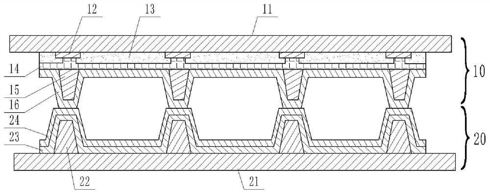
[0094] Such as Figure 17 As shown, the package cover plate 10 provided in this embodiment includes a plurality of auxiliary electrode units, and each auxiliary electrode unit can be arranged in an array, wherein the auxiliary electrode unit includes both the first auxiliary electrode unit 17 in Embodiment 1 and the first auxiliary electrode unit 17 in Embodiment 2. The second auxiliary electrode unit 18 in. That is, the first auxiliary electrode unit 17 includes a light guide column 171 and a first auxiliary electrode 172. The light guide column 171 is formed on the surface of the flat layer 14 and corresponds to the position of the color filter layer 13, and is far away from the flat layer. The width in the direction of 14 tapers to form inclined sidewalls; the first auxiliary electrode 172 is located in the gap between adjacent light guide columns 171, and has a first segment 1721 formed on the surface of the flat layer 14 corresponding to the position of the black matrix 1...
PUM
| Property | Measurement | Unit |
|---|---|---|
| Height dimension | aaaaa | aaaaa |
| Thickness | aaaaa | aaaaa |
| Height | aaaaa | aaaaa |
Abstract
Description
Claims
Application Information
 - R&D Engineer
- R&D Manager
- IP Professional
- Industry Leading Data Capabilities
- Powerful AI technology
- Patent DNA Extraction
Browse by: Latest US Patents, China's latest patents, Technical Efficacy Thesaurus, Application Domain, Technology Topic.
© 2024 PatSnap. All rights reserved.Legal|Privacy policy|Modern Slavery Act Transparency Statement|Sitemap