

Multi-mode switching circuit and control method thereof
A conversion circuit, multi-mode technology, used in control/regulation systems, output power conversion devices, electrical components, etc.
- Summary
- Abstract
- Description
- Claims
- Application Information
AI Technical Summary
Problems solved by technology
Method used
Image

Examples
Embodiment Construction
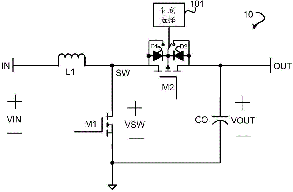
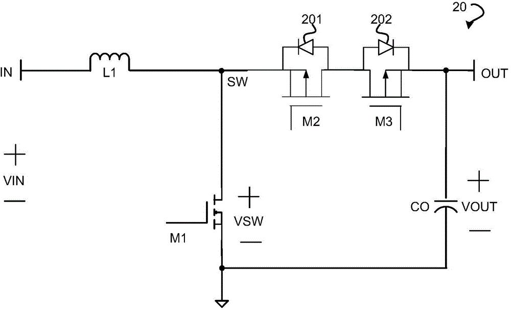
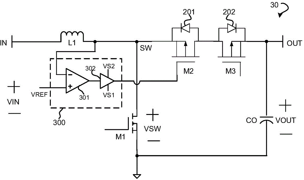
[0017] The specific embodiments described below represent exemplary embodiments of the invention and are merely illustrative rather than limiting in nature. In the specification, reference to "one embodiment" or "an embodiment" means that a particular feature, structure, or characteristic described in connection with the embodiment is included in at least one embodiment of the present invention. The appearances of the term "in one embodiment" in various places in the specification are not all referring to the same embodiment, nor are they intended to mutually exclude other or alternative embodiments. All features disclosed in this specification, or steps in all methods or processes disclosed, may be combined in any manner, except for mutually exclusive features and / or steps.
[0018] Specific embodiments of the present invention will be described in detail below with reference to the accompanying drawings. Like reference numerals refer to like parts or features throughout the...
PUM
 Abstract
Description
Claims
Application Information