mems device and method of forming the same
A device and dielectric layer technology, which is applied in the field of MEMS devices and their formation, can solve the problems of low integration, large size, and inability to meet portability of micro-electromechanical devices, so as to improve the electrical isolation effect, the formation process is simple, and the integration is improved. degree of effect
- Summary
- Abstract
- Description
- Claims
- Application Information
AI Technical Summary
Problems solved by technology
Method used
Image
Examples
no. 1 example
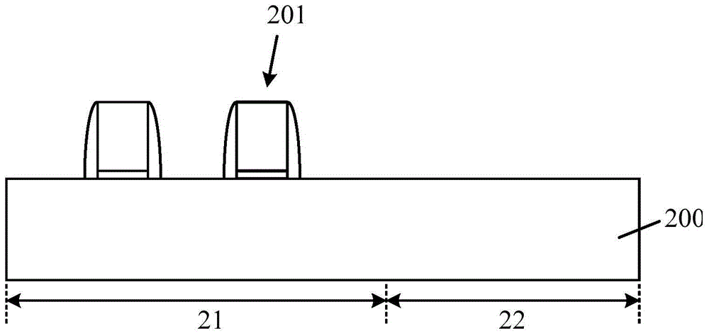
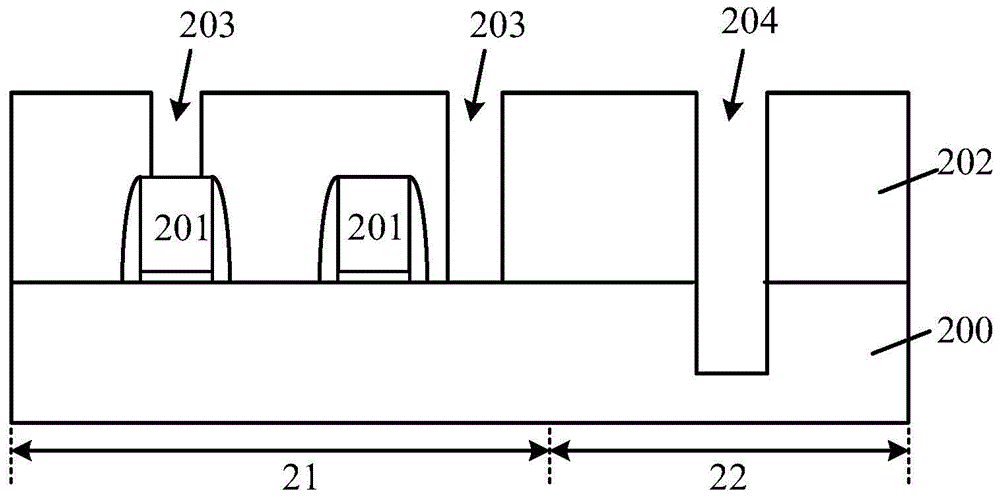
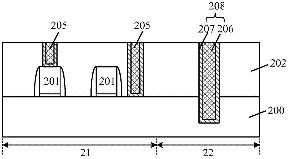
[0035] Figure 1 to Figure 7 It is a schematic cross-sectional structure diagram of the formation process of the MEMS device according to the first embodiment of the present invention.
[0036] refer to figure 1, providing a semiconductor substrate 200 having a first region 21 and a second region 22 ; forming a CMOS device 201 on the front side of the semiconductor substrate 200 in the first region 21 .
[0037] The material of the semiconductor substrate 200 may be silicon (Si), germanium (Ge), or silicon germanium (GeSi), silicon carbide (SiC); it may also be silicon on insulator (SOI), germanium on insulator (GOI); Or it can also be other materials, such as III-V group compounds such as gallium arsenide. In this embodiment, the semiconductor substrate 200 is a silicon substrate.
[0038] The semiconductor substrate 200 includes a first region 21 and a second region 22 , the first region 21 is used to form a CMOS device, and the second region 22 is used to form a via inte...
no. 2 example
[0081] Figure 8 ~ Figure 13 It is a schematic cross-sectional structure diagram of the formation process of the MEMS device according to the second embodiment of the present invention.
[0082] refer to Figure 8 , providing a semiconductor substrate 300 having a first region 31 and a second region 32; forming a CMOS device 301 on the front side of the semiconductor substrate 300 in the first region 31; forming a layer covering the semiconductor substrate 300 and the dielectric layer of the CMOS device 301, the dielectric layer includes a first dielectric layer 302 and a second dielectric layer 315, a first interconnection structure 311 is formed in the dielectric layer of the first region 31, and the first plug 305 serves as the first A part of the interconnection structure 311, the first interconnection structure 311 is connected to the CMOS device 301, the second interconnection structure 314 is formed in the dielectric layer of the second region 32; the first interconnec...
PUM
 Abstract
Description
Claims
Application Information


