Counterpoint label, circuit board and display device

一种对位标识、电路板的技术,应用在电路板工具定位、印刷电路、印刷电路等方向,能够解决无法满足电路板窄边化要求、降低电路板利用率等问题,达到满足窄边化、提高利用率的效果

Inactive Publication Date: 2015-05-27
BOE TECH GRP CO LTD
View PDF3 Cites 19 Cited by
  • Summary
  • Abstract
  • Description
  • Claims
  • Application Information

AI Technical Summary

Problems solved by technology

[0003] In order to solve the above problems, the present invention provides an alignment mark, a circuit board and a display device, which are used to solve the problems in the prior art that the alignment mark reduces the utilization rate of the circuit board and cannot meet the requirements of narrowing the edge of the circuit board

Method used


Image

  • Counterpoint label, circuit board and display device
  • Counterpoint label, circuit board and display device
  • Counterpoint label, circuit board and display device

Examples


Embodiment 1

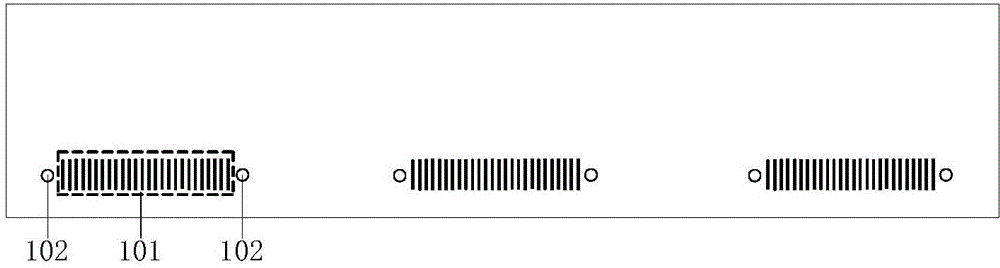
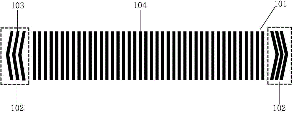
[0023] image 3 It is a schematic structural diagram of an alignment mark provided by Embodiment 1 of the present invention. Such as image 3 As shown, the alignment mark 102 is set on the binding area 101, and the alignment mark 102 is used to locate the parts to be bound during the binding process, and the alignment mark 102 is set on the parts to be bound The first gold finger 103 on the top constitutes. A plurality of second golden fingers 104 spaced apart from each other are also arranged on the binding area 101 . Optionally, there are two alignment marks 102 in one binding area 102, wherein one alignment mark 102 is set at one end of the binding area 101, and the other alignment mark 102 is set at the end of the binding area 101. The other end of the binding area 101.

[0024] In practical applications, the components to be bound include flexible circuit boards or printed circuit boards. Gold Finger (Gold Finger) is the interface between the circuit of the printed c...

Embodiment 2

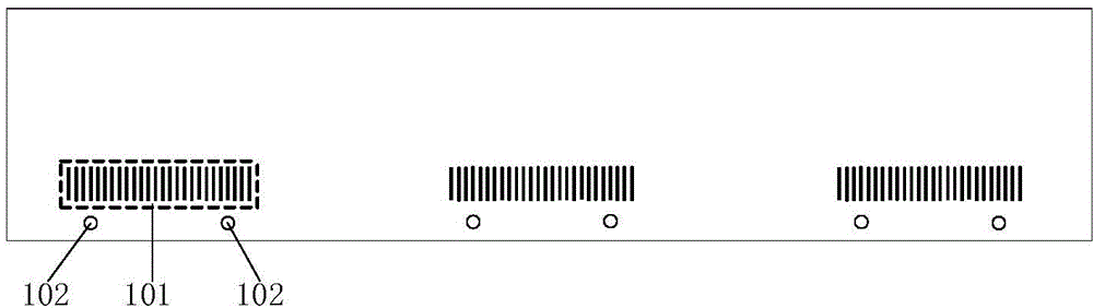
[0028] Figure 5 It is a schematic structural diagram of a circuit board provided by Embodiment 2 of the present invention. see image 3 and Figure 5 , the circuit board includes a substrate 105, and the substrate 105 is provided with a binding area 101, and the binding area 101 is provided with the alignment mark 102 provided in the first embodiment. The alignment mark 102 is used for positioning the components to be bound during the binding process, and the alignment mark 102 is composed of a first golden finger 103 arranged on the components to be bound. A plurality of second golden fingers 104 spaced apart from each other are also arranged on the binding area 101 . Optionally, there are two alignment marks 102 in one binding area 102, wherein one alignment mark 102 is set at one end of the binding area 101, and the other alignment mark 102 is set at the end of the binding area 101. The other end of the binding area 101.

[0029] In practical applications, the compone...

Embodiment 3

[0033] This embodiment provides a display substrate, including the circuit board provided in Embodiment 2. For specific content, refer to the description in Embodiment 2 above, which will not be repeated here.

[0034] In the display device provided in this embodiment, the alignment mark is used to position the component to be bound during the binding process, and the alignment mark is formed by a first golden finger arranged on the component to be bound. The alignment mark provided by this embodiment is set in the binding area without additionally occupying the effective area of ​​the circuit board, so that more components can be placed on the circuit board, thereby improving the utilization rate of the circuit board and meeting the requirements of narrowing the circuit board Require.


PUM


Abstract

The invention discloses a counterpoint label, a circuit board and a display device. The counterpoint label is used for positioning a component to be bound in the binding process; the counterpoint label consists of a first golden finger arranged on the component to be bound. The counterpoint label disclosed by the invention is arranged inside a binding area, so that effective areas of the circuit board are not additionally occupied, relatively more elements and components can be placed on the circuit board, the utilization rate of the circuit board can be increased, and the requirement of narrowing the side of the circuit board can be met.

Description

technical field [0001] The invention relates to the technical field of integrated electric boards, in particular to an alignment mark, a circuit board and a display device. Background technique [0002] figure 1 It is a structural schematic diagram of an alignment mark in the prior art. Such as figure 1 As shown, the alignment mark 102 is set on both sides of the binding area 101 . figure 2 It is a structural schematic diagram of another alignment mark in the prior art. Such as figure 2 As shown, the alignment mark 102 is set under the binding area 101 . The above-mentioned alignment mark is set on the bottom or both sides of the binding area, so that other components can not be set in the area where the alignment mark is set, which will waste a part of the circuit board area, thereby reducing the utilization rate of the circuit board, and making the circuit The volume of the board is too large, which cannot meet the requirements of narrowing the circuit board. Con...

Claims


Application Information

Patent Timeline
Patent Type & Authority Applications(China)
IPC IPC(8): H05K1/11G09F9/30
CPCG09F9/30H05K3/0008H05K1/111H05K2201/09918H05K2203/166H05K1/0269Y02P70/50H05K5/0017
Inventor 王铁石滕万鹏
Owner BOE TECH GRP CO LTD
Why Eureka
Try Eureka