Method for detecting electric charge damage in photolithography technique

A lithography process and a technology for detecting light, which are applied in microlithography exposure equipment, photolithography exposure devices, circuits, etc., can solve problems such as poor chemical reagent spit, excessive wafer speed, and reliability risks. Achieve convenient and timely effective charge damage, improve yield and reliability, and optimize photolithography process conditions

Active Publication Date: 2015-06-03
SHANGHAI HUAHONG GRACE SEMICON MFG CORP
View PDF3 Cites 0 Cited by
  • Summary
  • Abstract
  • Description
  • Claims
  • Application Information

AI Technical Summary

Problems solved by technology

Normally, the charge generated on the surface of the wafer will be released through the ionic conduction in the chemical reagent, but sometimes due to improper setting of photolithography conditions, such as too fast wafer speed, or poor spit of chemical reagents, the surface of the wafer will be damaged. Local charge accumulation, causing local strong electrochemical reactions in the subsequent wet process, causing damage on the wafer surface (see figure 1 ), causing circuit failure or reduced reliability, resulting in reduced yield or reliability risk
[0003] After the existing photolithography process is completed, usually only the feature size (CD) and misalignment (misalignment) are measured to meet the requirements, but there is no convenient means to detect the charge accumulation and damage introduced by the photolithography process, so it is difficult to find out in time , it is even more difficult to assess the degree of charge damage, and it is often found in the final step of chip manufacturing - electrical testing. At this time, not only the chip is scrapped, but the time cost caused cannot be compensated

Method used


Image

  • Method for detecting electric charge damage in photolithography technique
  • Method for detecting electric charge damage in photolithography technique
  • Method for detecting electric charge damage in photolithography technique

Examples


Embodiment Construction

[0033] The present invention will be described in further detail below in conjunction with the accompanying drawings and embodiments.

[0034] The invention discloses a method for detecting charge damage in a photolithography process. The method can be applied to a semiconductor process followed by a wet process after photolithography. The method specifically includes the following steps:

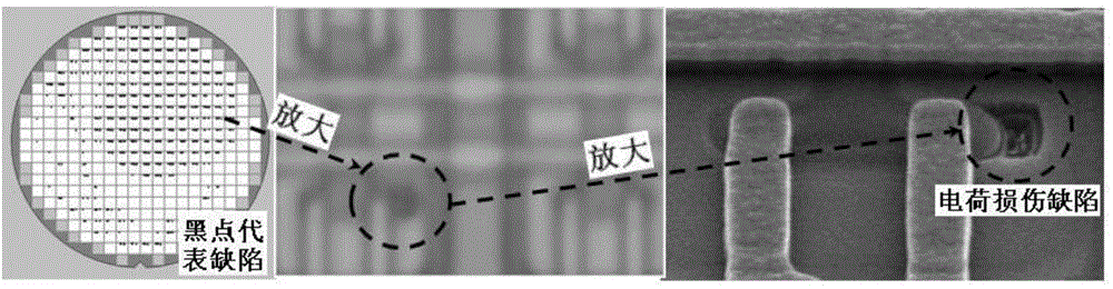
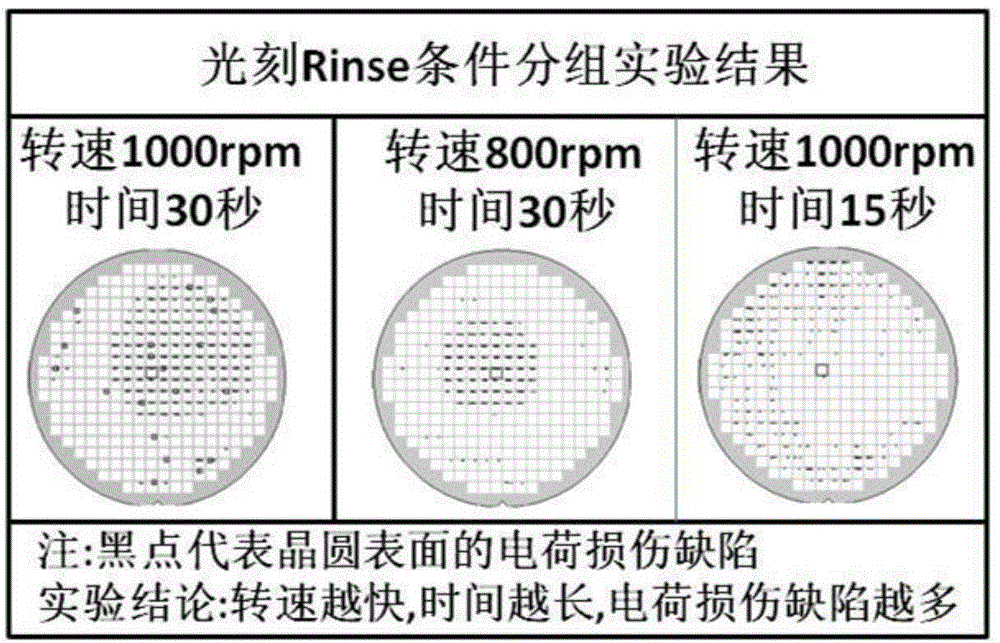
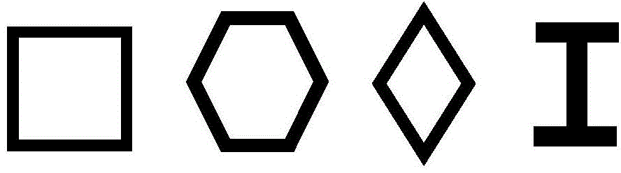
[0035] Step 1: When designing the product layout, place the detection pattern in the chip or dicing groove (the detection pattern can be placed in the chip (affecting wafer utilization, not recommended), or in the dicing groove (recommended) ). The detection pattern is given by image 3 Cell arrays consisting of repeating arrangements of detection cells are shown, such as Figure 4 , Figure 5 , Figure 6 and Figure 7 shown. The unit structure of the detection figure can be a circle, an I-shape, or a polygon. Such as image 3 As shown, the unit structure of the detection pattern ca...


PUM

PropertyMeasurementUnit
areaaaaaaaaaaa

Abstract

The invention discloses a method for detecting electric charge damage in a photolithography technique. The method comprises the following steps: S1, adding a detection graph in a chip or a scribe line during chip design; S2, preparing a corresponding photolithography mask; S3, performing the photolithography technique by using the photolithography mask with the detection graph, and accumulating electric charges in the detection graph area; S4, performing wet processing; S5, performing defect detection on the detection graph and evaluating the electric charge damage in the photolithography technique. By adopting method disclosed by the invention, the electric charge damage generated by the photolithography technique can be conveniently and effectively evaluated in time, so that defects existing in the condition of the photolithography technique are found and optimized as soon as possible, the fault of photolithography equipment is found and removed as soon as possible, and the chip yield and the reliability of the chip are improved.

Description

technical field [0001] The invention belongs to the field of semiconductor integrated circuit manufacturing, and in particular relates to a detection method in the semiconductor integrated circuit manufacturing, in particular to a method for detecting charge damage in a photolithography process. Background technique [0002] Photolithography is a common process in the manufacture of semiconductor integrated circuits. During the photolithography process, chemical solvents such as developers rub against the surface of the rotating wafer to generate charges. Normally, the charge generated on the surface of the wafer will be released through the ionic conduction in the chemical reagent, but sometimes due to improper setting of photolithography conditions, such as too fast wafer speed, or poor spit of chemical reagents, the surface of the wafer will be damaged. Local charge accumulation, causing local strong electrochemical reactions in the subsequent wet process, causing damage...

Claims


Application Information

Patent Timeline
Patent Type & Authority Applications(China)
IPC IPC(8): H01L21/66G03F7/20
CPCG03F7/20H01L22/10
Inventor 沈今楷李亮刘春玲
Owner SHANGHAI HUAHONG GRACE SEMICON MFG CORP
Why Eureka
Try Eureka