Public voltage adjustment method, adjustment device, and display device

A common voltage and adjustment method technology, applied to static indicators, instruments, etc., can solve problems such as poor flicker uniformity, affecting display effect, and small flicker in the central area

Inactive Publication Date: 2017-03-29
BOE TECH GRP CO LTD +1
View PDF5 Cites 0 Cited by
  • Summary
  • Abstract
  • Description
  • Claims
  • Application Information

AI Technical Summary

Problems solved by technology

[0008] However, the inventors of the present application found that the common voltage value obtained by using the above method has the following problems in the final display: the flickering in the central area of ​​the display panel is small, while the flickering in the edge area is serious, and the flickering uniformity is poor, which affects the display effect

Method used


Image

  • Public voltage adjustment method, adjustment device, and display device
  • Public voltage adjustment method, adjustment device, and display device
  • Public voltage adjustment method, adjustment device, and display device

Examples


Embodiment 1

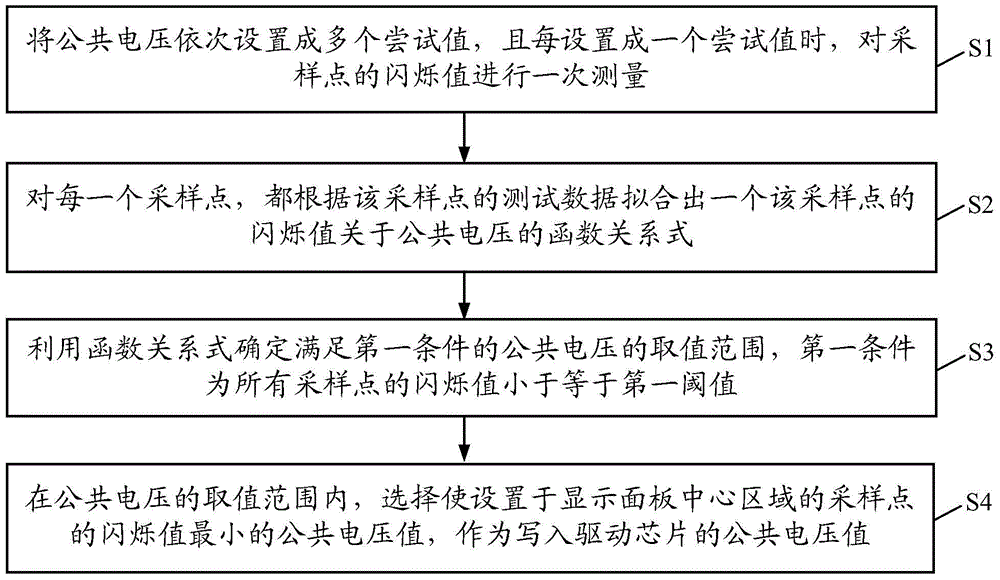
[0067] This embodiment provides a public voltage regulation method, including:

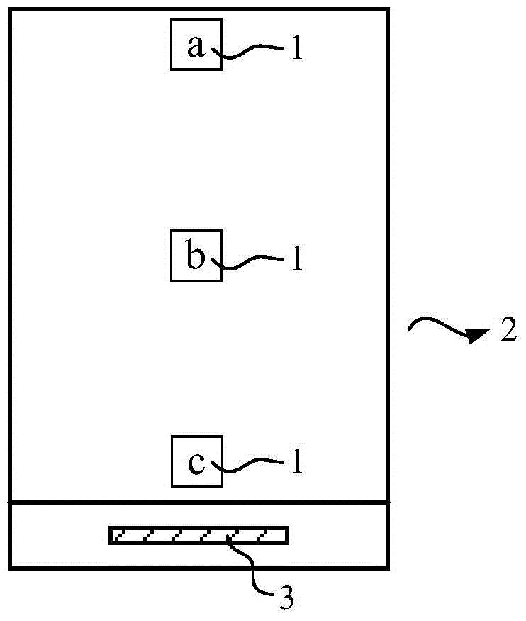
[0068] Step 1, setting sampling points, the sampling points at least include: sampling points set in the center area of ​​the display panel and sampling points set in the edge area of ​​the display panel.

[0069] In the public voltage adjustment method provided in this implementation, the flicker level of the area where the sampling point is located is obtained by measuring the flicker value of the sampling point. One sampling point is set in the center area and the edge area respectively. The more sampling points, the more uniform the distribution on the display panel, and the more consistent the flicker after step 2 common voltage optimization setting, but it also means that the step 2 common voltage optimization setting is more difficult and the amount of calculation is greater, so generally speaking, as long as the flickering It is sufficient to set sampling points in representative areas of...

example 1

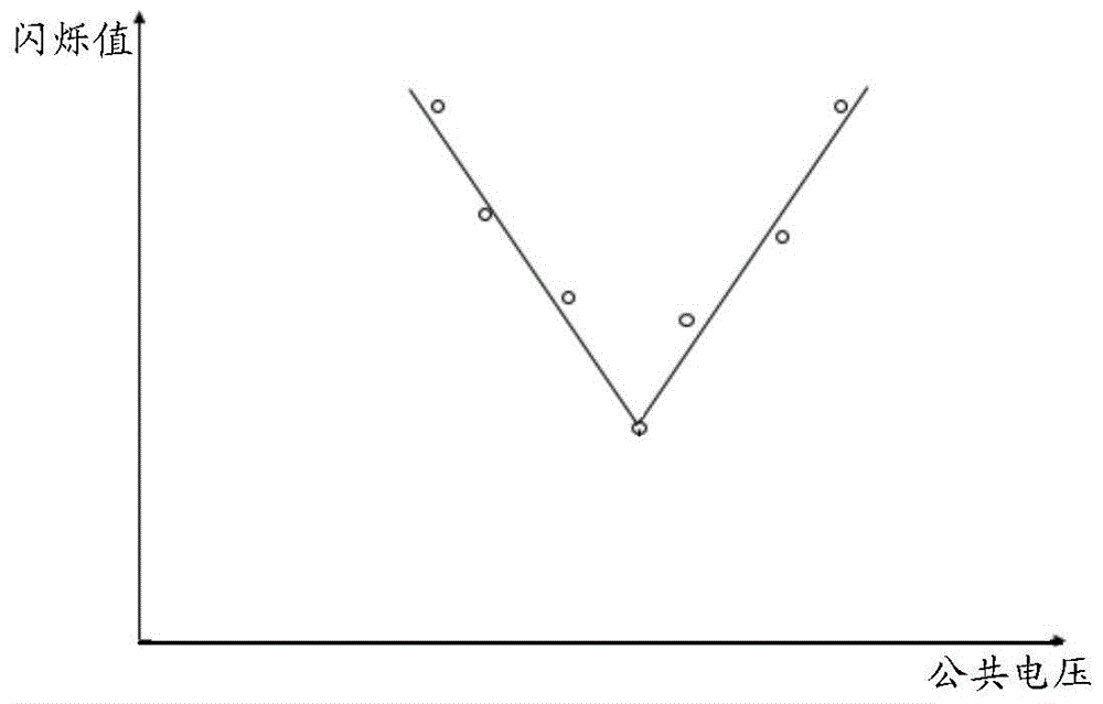
[0113] Example 1, the process of this example is as follows Figure 6 As shown, in this example, the setting of sampling points on the display panel is as follows figure 1 shown. In step S1, test data of sampling points a, b, and c are obtained. In step S2, according to the test data fitting of the sampling point, a piecewise linear function relational expression corresponding to each sampling point is obtained, specifically as Figure 4 As shown, the curves A, B, and C represent respectively figure 1 The functional relationship expressions y1(x), y2(x), y3(x) corresponding to the sampling points a, b, and c in . Step S3 is specifically as follows:

[0114] First, step S31 presets the values ​​P1 and P2 of two flicker values, and P1

[0115] Step S32 For the given value of P1, calculate the solution of the inequality group: y1(x)≤P1, y2(x)≤P1, y3(x)≤P1, if there is a solution, that is, X1≤x≤X2, then this The range is defined as the first value ran...

Embodiment 2

[0124] This embodiment provides a common voltage adjustment device. The common voltage adjustment device is used to optimize the common voltage value written into the drive chip, so that when the display panel is loaded with the common voltage value for display, the flicker value of the sampling point on the display panel All are less than or equal to the first threshold, and the sampling points at least include: sampling points set in the center area of ​​the display panel and sampling points set in the edge area of ​​the display panel.

[0125] The common voltage adjusting device of this embodiment is used to implement the common voltage adjusting method in the first embodiment, optimize the written value of the common voltage of the drive chip, and when the display panel loads the written value of the common voltage optimized by the embodiment of the present invention for display, Not only the flicker in the center area is smaller, but also the flicker in the edge area is ef...


PUM


Abstract

A method for regulating a common voltage, a regulating device and a display device. It relates to the display field, which ensures the flicker in the center region of the display panel being relative small meanwhile improving the flicker situation of the edge region of the display panel, thereby improve the flicker uniformity of the display panel. The present disclosure provides a method for regulating a common voltage including: arranging sampling points which at least include: sampling points arranged in the center region of the display panel and sampling points arranged in the edge region of the display panel; optimizing the common voltage value written into the driving chip, such that the flicker values of the sampling points located in the display panel are less than or equal to a first threshold when the common voltage value is applied to the display panel for display.

Description

technical field [0001] The invention relates to the display field, in particular to a public voltage regulation method, regulation device, and display device. Background technique [0002] The liquid crystal cell of the liquid crystal display is formed by pressing two glass substrates. The two glass substrates are respectively provided with an alignment film for guiding the alignment of the liquid crystal. Due to the DC blocking effect of the alignment film and the DC residual caused by the movable ions in the liquid crystal cell pressure, resulting in poor display such as afterimages in the display process of the LCD monitor. In order to solve the poor display caused by the above reasons, the liquid crystal display usually adopts a polarity inversion driving method. [0003] When the liquid crystal display adopts the polarity inversion driving mode to display, the thin film transistor that controls the loading of the pixel display signal has a parasitic capacitance effect ...

Claims


Application Information

Patent Timeline
Patent Type & Authority Patents(China)
IPC IPC(8): G09G3/36
CPCG09G3/3696G09G3/006G09G3/20G09G3/3648G09G2320/0247G09G2320/045
Inventor 丁金波王静李鑫张莹朱红于洪俊
Owner BOE TECH GRP CO LTD
Why Eureka
Try Eureka