An organic light emitting diode display with a touch panel

A technology of light-emitting diodes and touch panels, applied in instruments, semiconductor devices, electric solid-state devices, etc., can solve problems such as input errors and waste of light energy, and achieve the effect of reducing failures, reducing impacts, and realizing self-charging

Active Publication Date: 2018-05-29
GUANGZHOU GOVISIONOX TECH CO LTD
View PDF5 Cites 1 Cited by
  • Summary
  • Abstract
  • Description
  • Claims
  • Application Information

AI Technical Summary

Problems solved by technology

[0004] The technical problem to be solved by the present invention is that the light sensor of an OLED display with a touch panel itself will be affected by the light emission of the internal OLED in the OLED device, and malfunction, resulting in input errors and wasting light energy

Method used


Image

  • An organic light emitting diode display with a touch panel
  • An organic light emitting diode display with a touch panel
  • An organic light emitting diode display with a touch panel

Examples


Embodiment 1

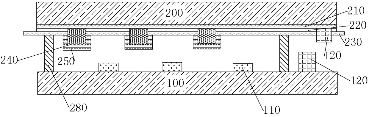
[0028] combine figure 1 As shown, it is a cross-sectional view of an organic light emitting diode display with a touch panel in this embodiment. The organic light emitting diode display with touch panel of the present embodiment includes:

[0029] The first substrate 100, a plurality of organic light emitting diode pixel units 110 provided in the display area of ​​the first substrate 100, combined (attached or connected) with the first substrate 100 through the sealing unit 280 (which may be a bonding agent, etc.) The second substrate 200, the touch electrode 210 formed on the second substrate 200 (the side facing the first substrate 100), the transparent insulating layer 220 formed on the touch electrode 210, the conductive layer 230 formed on the transparent insulating layer 220 , a plurality of photosensors 240 and a plurality of photovoltaic material layers 250 . The corresponding positions of the transparent insulating layer 220 and the conductive layer 230 are formed w...

Embodiment 2

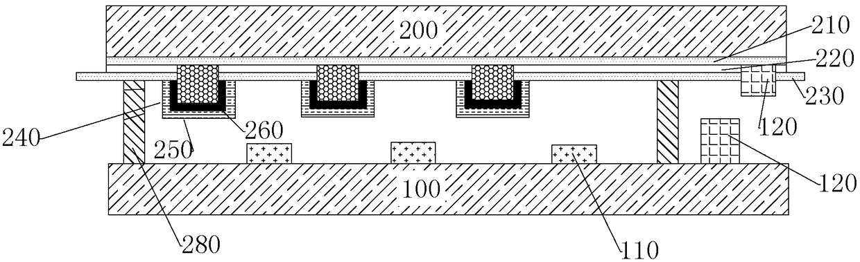
[0045] Such as figure 2 As shown, it is a cross-sectional view of an OLED display with a touch panel in this embodiment. This embodiment is basically the same as Embodiment 1, the difference being that the organic light emitting diode display with a touch panel of this embodiment is further provided with a reflective layer 260 between the photovoltaic material layer 250 and the light sensor 240 .

[0046] Specifically, combined with figure 2 , the organic light emitting diode display with touch panel of this embodiment includes:

[0047] the first substrate 100;

[0048] OLED pixel unit 110, located on the first substrate 100;

[0049] a second substrate 200, which is connected to the first substrate 100 through a sealing unit 280;

[0050] The touch electrode 210 is located on the second substrate 200;

[0051] a transparent insulating layer 220 formed on the touch electrode 210;

[0052] The conductive layer 230 is formed on the transparent insulating layer 210, and ...


PUM


Abstract

The invention discloses an organic light emitting diode display with a touch panel, comprising: a first substrate; an organic light emitting diode pixel unit located on the first substrate; a second substrate connected to the first substrate; a touch electrode located on the second substrate On the second substrate; a transparent insulating layer, formed on the touch electrode; a conductive layer, formed on the transparent insulating layer; a photosensor for detecting incident light generated by an external source, which is formed on the corresponding positions of the transparent insulating layer and the conductive layer. The through hole is located on the touch electrode; the photovoltaic material layer shields the surface of the light sensor on the side of the conductive layer facing the first substrate, and the photovoltaic material layer is coupled with the conductive layer. The photovoltaic material layer provided by the invention prevents the light emitted by the OLED from being detected by the light sensor, reduces the influence of the OLED light on the light sensor, and can absorb the light emitted by the OLED and convert it into electrical energy for self-power generation to realize self-charging of terminal products.

Description

technical field [0001] The invention relates to the field of organic light emitting diode displays, in particular to an organic light emitting diode display with a touch panel. Background technique [0002] For organic light-emitting diode (OLED) displays and their products, convenient and fast input can be performed through the touch screen, which becomes a new input method to replace existing input methods (such as keyboard and mouse). According to different implementation methods, touch screen can be divided into: resistive film method, capacitive method or light (infrared) method, etc.; the so-called resistive film method needs to realize input by pressing or touching and sliding the screen surface, which is easy to damage the display panel. [0003] The so-called optical method is provided by a light sensor to detect changes in incident light and generate a corresponding electrical signal, and detect the position based on the electrical signal. According to this method,...

Claims


Application Information

Patent Timeline
Patent Type & Authority Patents(China)
IPC IPC(8): H01L27/32G06F3/042
Inventor 李南征苟琦王磊程保龙卜维亮
Owner GUANGZHOU GOVISIONOX TECH CO LTD
Why Eureka
Try Eureka