Detection circuit of array substrate and array substrate

An array substrate and circuit technology, applied in the field of liquid crystal display, can solve the problems of high height, large frame of liquid crystal display, excessive detection circuit area, etc., and achieve the effect of low height and small occupied area

Active Publication Date: 2015-07-08
SHENZHEN CHINA STAR OPTOELECTRONICS TECH CO LTD +1
View PDF5 Cites 7 Cited by
  • Summary
  • Abstract
  • Description
  • Claims
  • Application Information

AI Technical Summary

Problems solved by technology

[0003] However, the existing array substrate detection circuit has the defect that the height is too high, which makes the area occupied by the detection circuit too large
Since the detection cir

Method used


Image

  • Detection circuit of array substrate and array substrate
  • Detection circuit of array substrate and array substrate
  • Detection circuit of array substrate and array substrate

Examples


Embodiment Construction

[0029] The implementation of the present invention will be described in detail below with reference to the accompanying drawings and embodiments, so as to fully understand how the present invention applies technical means to solve technical problems and achieve the realization process of technical effects and implement them accordingly. It should be noted that, as long as there is no conflict, each embodiment of the present invention and each feature in each embodiment can be combined with each other, and the technical solutions formed are all within the protection scope of the present invention.

[0030] Meanwhile, in the following description, many specific details are set forth for the purpose of explanation to provide a thorough understanding of the embodiments of the present invention. However, it is obvious to those skilled in the art that the present invention may be implemented without the specific details or the specific manner described herein.

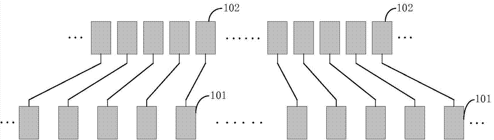
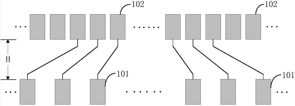
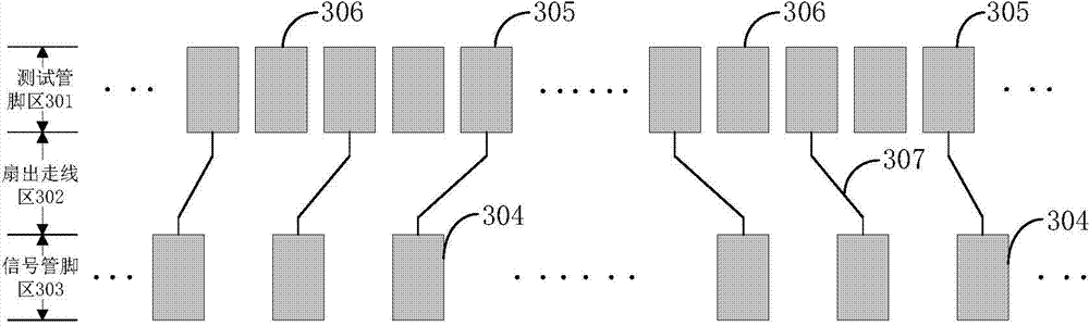
[0031] Since there are li...


PUM


Abstract

The invention provides a detection circuit of an array substrate and the array substrate. The detection circuit comprises a signal pin area, a test pin area and a fan-out wiring area, wherein the signal pin area include multiple signal pins, the signal pins are correspondingly connected with signal lines in the array substrate, the test pin area include multiple testing pins, the fan-out wiring area is connected between the signal pin area and the test pin area and comprises multiple fan-out wires, the signal pins are connected to a part of testing pins through the fan-out wires and are not mutually adjacent to the test pins connected with the signal pins, and accordingly the height of the fan-out wiring area is decreased.

Description

Technical field [0001] The present invention relates to the technical field of liquid crystal display, in particular to a detection circuit of an array substrate and an array substrate. Background technique [0002] Generally, in the process of fabricating the array substrate of the liquid crystal display, an epitaxial method is used to form millions of thin film transistors as the control unit on the array substrate of the liquid crystal display. However, in the production process of array substrates, if the quality of some thin film transistors does not meet the preset requirements, these thin film transistors may not have the function of switching control, so that the liquid crystal display has a bright or dark curve. Decrease the quality of the LCD display. Therefore, during the production process of the array substrate, the array substrate must be inspected effectively to ensure the quality of the array substrate. [0003] However, the detection circuit of the existing array...

Claims


Application Information

Patent Timeline
IPC IPC(8): G02F1/13
CPCG02F1/1362G02F1/136254G02F1/133
Inventor 田勇赵莽
Owner SHENZHEN CHINA STAR OPTOELECTRONICS TECH CO LTD
Why Eureka
Try Eureka