Printed circuit board and method of manufacturing the same

A technology of printed circuit boards and pathways, applied in the field of printed circuit boards and its manufacturing, can solve the problems of increased time from order to delivery, etc., achieve the effect of reducing the time from order to delivery, increasing the degree of freedom, and eliminating the phenomenon of sag

Active Publication Date: 2015-08-19
LG INNOTEK CO LTD
View PDF7 Cites 1 Cited by
  • Summary
  • Abstract
  • Description
  • Claims
  • Application Information

AI Technical Summary

Problems solved by technology

However, if the plating process is performed several times, the lead time of the product may increase

Method used


Image

  • Printed circuit board and method of manufacturing the same
  • Printed circuit board and method of manufacturing the same
  • Printed circuit board and method of manufacturing the same

Examples


Embodiment Construction

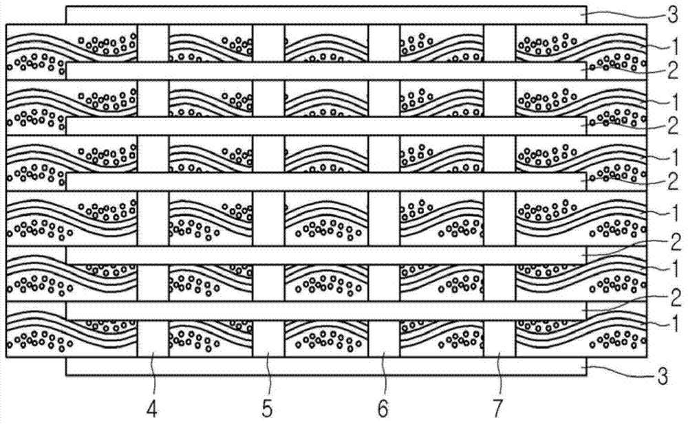
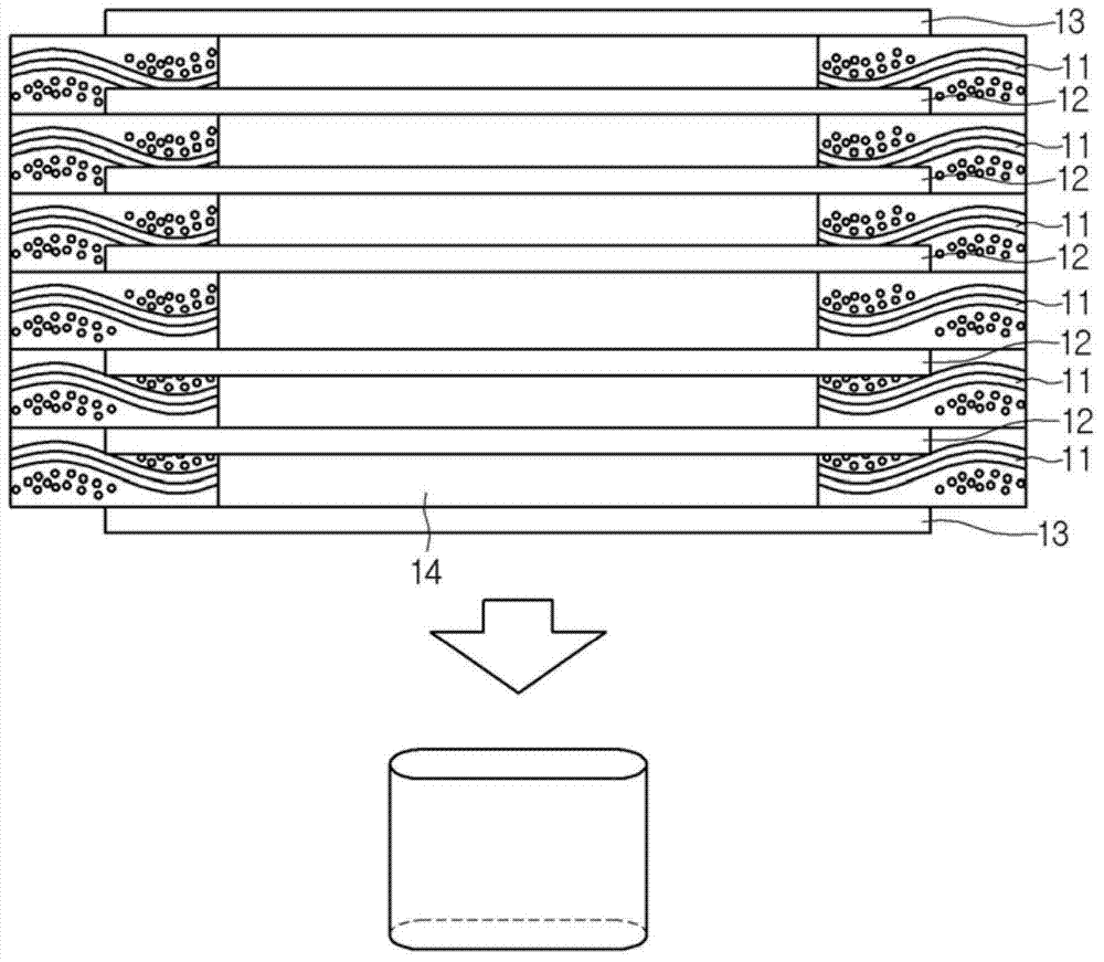
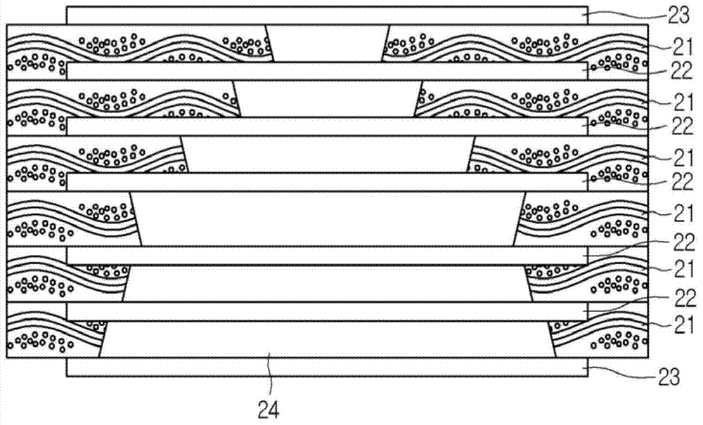
[0064] Hereinafter, the embodiments will be described in detail with reference to the accompanying drawings so that those skilled in the art can easily utilize the embodiments. However, the embodiments are not limited to the above, but may have various modifications.

[0065] In the following description, when a predetermined part "includes" a predetermined element, the predetermined part does not exclude other elements, but may also include other elements, unless there is a specific description to the contrary.

[0066] The thickness and size of each layer shown in the drawings may be exaggerated, omitted, or schematically drawn for the purpose of convenience or clarity. Also, the size of elements does not utterly reflect an actual size. Like reference numerals will refer to like elements throughout the drawings.

[0067] In describing embodiments, it will be understood that when a layer, film, region, or panel is referred to as being "on" or "under" another layer, film, re...


PUM


Abstract

A printed circuit board according to the embodiment includes an insulating layer; a first pad on a top surface of the insulating layer; a second pad on a bottom surface of the insulating layer; and a via formed in the insulating layer and having one surface connected to the first pad and an opposite surface connected to the second pad, wherein the via includes a plurality of via parts which are at least partially overlapped with each other.

Description

[0001] Cross References to Related Applications [0002] This application claims the priority of Korean Patent Application No. 10-2014-0018131 (filed on February 17, 2014) and No. 10-2014-0020573 (filed on February 21, 2014). The entire contents of both are incorporated herein by reference. technical field [0003] The present disclosure relates to printed circuit boards and methods of manufacturing the same. Background technique [0004] A printed circuit board (PCB) is formed by printing a circuit pattern on an electrically insulating substrate using a conductive material such as copper (Cu), and refers to a board immediately before electronic components are mounted thereon. In other words, PCB refers to a circuit board in which the mounting positions of electronic parts are determined, and circuit patterns connecting electronic parts to each other are fixedly printed on the surface of a flat board, so that many electronic parts of several types are densely mounted on a f...

Claims


Application Information

Patent Timeline
Patent Type & Authority Applications(China)
IPC IPC(8): H05K1/02H05K1/11H05K3/46
CPCH05K2201/09854H05K1/0206H05K1/113H05K3/429Y10T29/49155H05K3/0044H05K2201/09618
Inventor 朴忠植金材华申铉乾
Owner LG INNOTEK CO LTD
Why Eureka
Try Eureka