Display substrate, manufacturing method of display substrate and display device

A technology for display substrates and display devices, which can be used in static indicators, light guides, optics, etc., and can solve the problems of large loss of brightness and energy

Active Publication Date: 2015-09-23
BOE TECH GRP CO LTD
View PDF6 Cites 11 Cited by
  • Summary
  • Abstract
  • Description
  • Claims
  • Application Information

AI Technical Summary

Problems solved by technology

[0005] In order to solve the problem of high light brightness and energy loss in the prior art, the

Method used


Image

  • Display substrate, manufacturing method of display substrate and display device
  • Display substrate, manufacturing method of display substrate and display device
  • Display substrate, manufacturing method of display substrate and display device

Examples


Embodiment Construction

[0115] In order to make the object, technical solution and advantages of the present invention clearer, the implementation manner of the present invention will be further described in detail below in conjunction with the accompanying drawings.

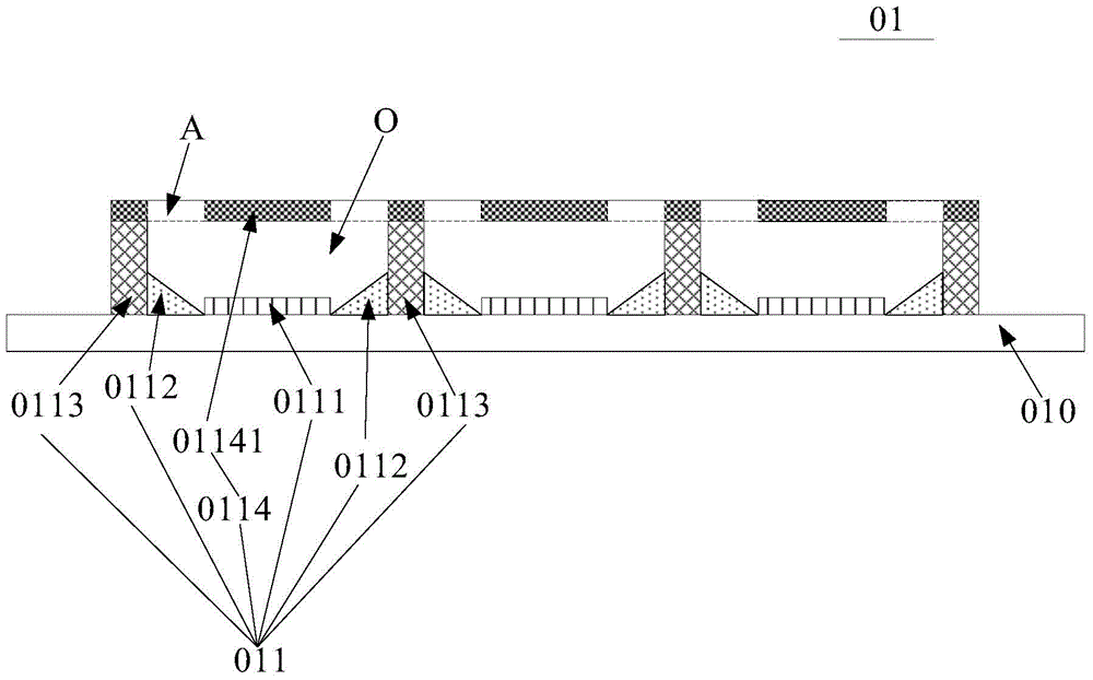
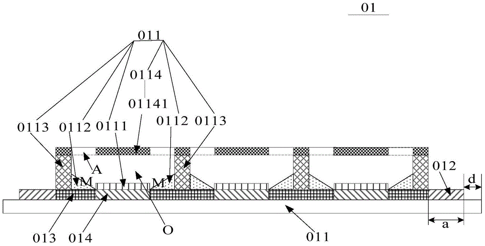
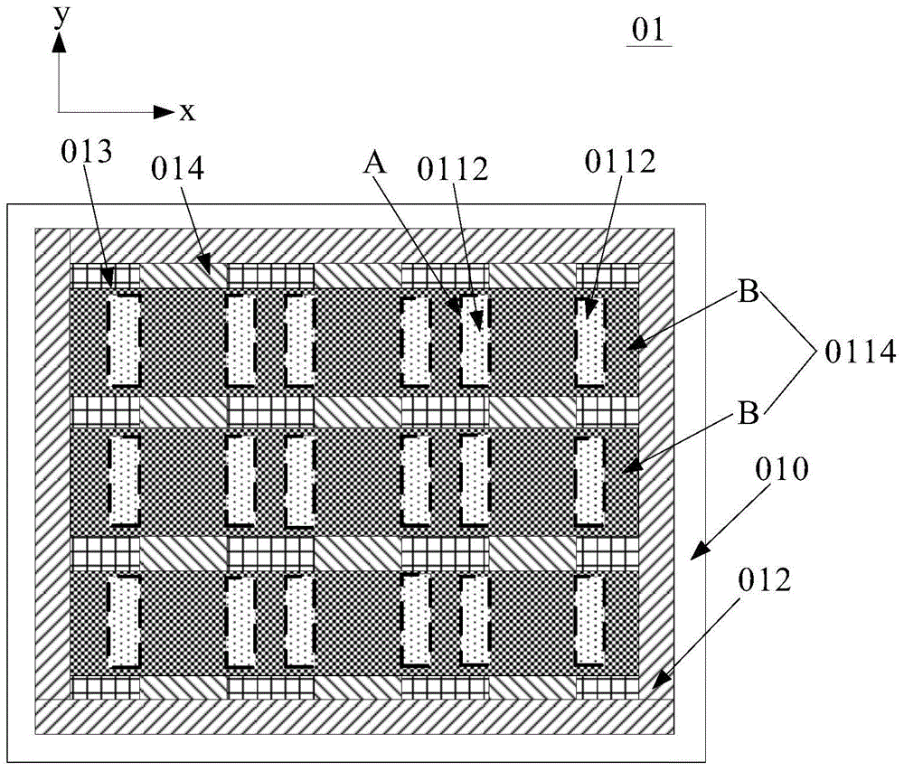
[0116] Please refer to figure 1 , which shows a schematic structural diagram of a display substrate 01 provided by an embodiment of the present invention. see figure 1 , the display substrate 01 includes: a base substrate 010, the base substrate 010 may be a transparent substrate, specifically, it may be a substrate made of light-guiding and non-metallic materials with certain firmness such as glass, quartz, and transparent resin.

[0117] At least one pixel unit 011 is formed on the display area of ​​the base substrate 010 .

[0118] Such as figure 1 As shown, each pixel unit 011 includes: a color-developing structure 0111, a first light-reflecting structure 0112 disposed around the color-developing structure 0111, disposed on at l...


PUM


Abstract

The invention discloses a displayer substrate, a manufacturing method of the display substrate and a display device and belongs to the technical field of display. The displayer substrate comprises a substrate base plate. A pixel unit is formed on the substrate base plate and comprises a color development structure, a first light-reflecting structure arranged on the periphery of the color development structure, a blocking structure arranged on the side face of the color development structure and located on the side, away from the color development structure, of the first light-reflecting structure, and a light-reflecting layer arranged on the blocking structure. A light transmission area and a second light-reflecting structure are formed on the light-reflecting layer, the orthographic projection of the light transmission area on the substrate base plate is located within the orthographic projection of the first light-reflecting structure on the substrate base plate, and the orthographic projection of the color development structure on the substrate base plate is located within the orthographic projection of the second light-reflecting structure on the substrate base plate. The color development structure, the first light-reflecting structure, the blocking structure and the light-reflecting structure form a cavity. Liquid crystal and a polarizer are not needed, light absorption of the liquid crystal and the polarizer is avoided, and the effects of reducing light brightness loss and saving energy are achieved.

Description

technical field [0001] The invention relates to the field of display technology, in particular to a display substrate, a manufacturing method thereof, and a display device. Background technique [0002] With the continuous development of display technology, display devices are widely used in the display field, and the existing display devices are usually liquid crystal displays (English: Liquid Crystal Display, LCD for short). [0003] LCDs usually use liquid crystal molecules to cooperate with polarizers to display images. Specifically, an LCD usually includes an array substrate and a color filter substrate formed in a cell, and a liquid crystal layer filled between the array substrate and the color filter substrate. The liquid crystal layer includes a plurality of liquid crystal molecules, and the backlight side of the array substrate is provided with an upper polarizer The light output side of the color filter substrate is provided with a lower polarizer, the backlight i...

Claims


Application Information

Patent Timeline
IPC IPC(8): G02F1/13357G02F1/1335G02F1/1343
CPCG02F1/133512G02F1/133605G02F1/134309G02B6/0031G02B6/0068G02B6/0088G02B6/009G02B26/001G02B26/02G09G3/2011G09G3/3433G02B6/0055G02F1/13439G09G3/2007G09G3/3611G09G2300/0426G09G2320/0271
Inventor 冯京
Owner BOE TECH GRP CO LTD
Why Eureka
Try Eureka