High voltage LED and production technology thereof

A manufacturing process and high-voltage technology, applied in electrical components, electric solid-state devices, circuits, etc., can solve problems such as brightness loss, and achieve the effect of reducing brightness loss and improving brightness

Inactive Publication Date: 2016-05-18
XIAMEN CHANGELIGHT CO LTD
View PDF3 Cites 2 Cited by
  • Summary
  • Abstract
  • Description
  • Claims
  • Application Information

AI Technical Summary

Problems solved by technology

However, this production technology has a loss of brightness due to N-PAD blocking the light emitted by the active area after the upper electrode is evaporated.

Method used


Image

  • High voltage LED and production technology thereof
  • High voltage LED and production technology thereof
  • High voltage LED and production technology thereof

Examples


Embodiment Construction

[0019] 1. Production process:

[0020] 1. The N-GaN layer, the quantum well layer and the P-GaN layer are sequentially grown on the same side of the sapphire substrate;

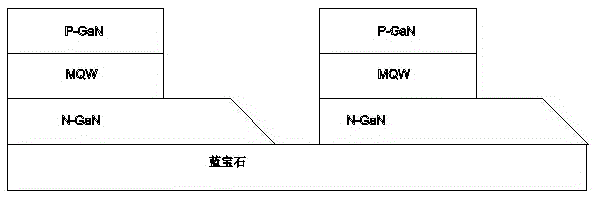
[0021] 2. In the yellow light lithography process, the P-GaN layer and part of the quantum well layer of each cell are etched and removed in a patterned manner by using induction couple and plasma (ICP), until the N-GaN layer is exposed, and the etching depth is about 10,000 ?~16000?, such as figure 2 shown.

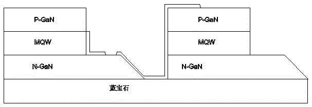
[0022] 3. On the basis of the N-GaN layer, use a thick photoresist with high resolution, and continue to use the etching induction couple and plasma (ICP) to adjust the ratio of etching gases BCl3 and Cl2, remove part of the N-GaN layer, etch The depth of etching is about 50000?~60000? until a part of the substrate is exposed to form a positive trapezoid with a side angle of about 130°~160°, such as image 3 shown.

[0023] 4. Evaporate a DBR layer with a thickness of about 3000~7000? The substrat...


PUM


Abstract

The invention discloses a high voltage LED and a production technology thereof, and relates to the LED production technology field. DBR layers are disposed on a surface of a semi-finished product by adopting the evaporation technology, and then after the etching treatment, the DBR layers on side walls of quantum wells and surfaces of N-GaN layers of all cells can be kept, and the DBR layers on the substrate surface, the side walls of the N-GaN layer, the side walls of the quantum well, the side walls of the P-GaN layer, and the surface of the P-GaN layer, which are arranged between the second electrode area of the cell and the first electrode area of another adjacent cell can be kept. The high voltage LED is characterized in that the DBR insulation layers can be arranged on the side walls of the quantum wells and the surfaces of the N-GaN layers of all cells, and the DBR layers can be arranged on the substrate surface, the side walls of the N-GaN layer, the side walls of the quantum wells, the side walls of the P-GaN layer, and the surface of the P-GaN layer, which are arranged between the second electrode area of one cell and the first electrode area of the adjacent cell. The light loss can be reduced, and then the brightness of the chip can be increased, when the DBR insulation functions are adopted by the cells.

Description

technical field [0001] The invention relates to the technical field of LED manufacture. Background technique [0002] The existing high-voltage chips produced industrially are formed by the arrangement and combination of multiple cells. In the current chip, CBL is used for insulation protection between the cells. Industrial production needs to be carried out in the second step of DE (deep etching to Insulation layer) After photolithography, CBL is evaporated to play the role of insulation protection. However, this production technology results in a loss of brightness due to the N-PAD blocking the light emitted by the active region after the top electrode is evaporated. Therefore, how to overcome the existing defects and improve the luminous efficiency is a problem to be solved by technicians. Contents of the invention [0003] The purpose of the present invention is to propose a high-voltage LED that overcomes the above defects of the prior art and can improve the bright...

Claims


Application Information

Patent Timeline
IPC IPC(8): H01L27/15H01L33/46H01L33/00
CPCH01L27/153H01L33/007H01L33/46H01L2933/0033
Inventor 蔡立鹤张永陈凯轩李俊贤刘英策陈亮魏振东吴奇隆周弘毅邬新根黄新茂
Owner XIAMEN CHANGELIGHT CO LTD
Why Eureka
Try Eureka