Chip information access method and device

An access method and chip technology, which is applied in the field of communication, can solve the problem of information in the chip being overwritten or erased, and achieve the effect of ensuring integrity and accurate positioning

Active Publication Date: 2015-09-30
GIGADEVICE SEMICON (BEIJING) INC
View PDF3 Cites 8 Cited by
  • Summary
  • Abstract
  • Description
  • Claims
  • Application Information

AI Technical Summary

Problems solved by technology

[0004] The technical problem to be solved by the embodiments of the present invention is to provide a chip information access method to solve the problem that the information in the chip is overwritten or erased

Method used


Image

  • Chip information access method and device
  • Chip information access method and device
  • Chip information access method and device

Examples


Embodiment 1

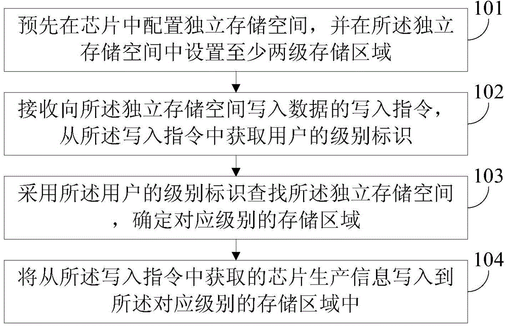
[0025] refer to figure 1 , which shows a flow chart of the steps of an embodiment of a method for accessing chip information in the present invention, which may specifically include the following steps:

[0026] Step 101, pre-configure an independent storage space in the chip, and set at least two levels of storage areas in the independent storage space.

[0027] In this embodiment, in order to prevent production information from being overwritten or tampered with during chip development, an independent storage space is configured in the chip. The independent storage space performs read and write operations.

[0028] Since the chip will be produced and developed by multiple users, such as the manufacturer of the chip, the manufacturer who makes the chip into a certain device, the person who develops the program in the chip, etc., at least two levels are set in this independent space storage area. The storage area of ​​each level stores information corresponding to users of ...

Embodiment 2

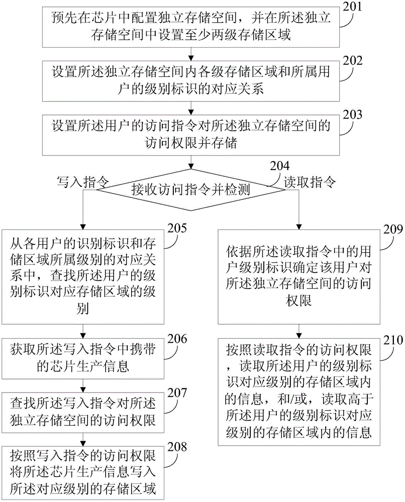
[0037] On the basis of the above embodiments, this embodiment continues to discuss the method for reading and writing access to chip information.

[0038] refer to figure 2 , which shows a flow chart of steps in an optional embodiment of a method for accessing chip information in the present invention, which may specifically include the following steps:

[0039] Step 201, pre-configure an independent storage space in the chip, and set at least two levels of storage areas in the independent storage space.

[0040] Step 202, setting the corresponding relationship between the storage areas of each level in the independent storage space and the level identifiers of the users to which they belong.

[0041]Step 203, setting and storing the access authority of the user's access instruction to the independent storage space.

[0042] In this embodiment, the storage areas in the independent storage space have priority, so that the storage areas in the independent storage space are st...

Embodiment 3

[0064] On the basis of the above embodiments, this embodiment also provides a device for accessing chip information.

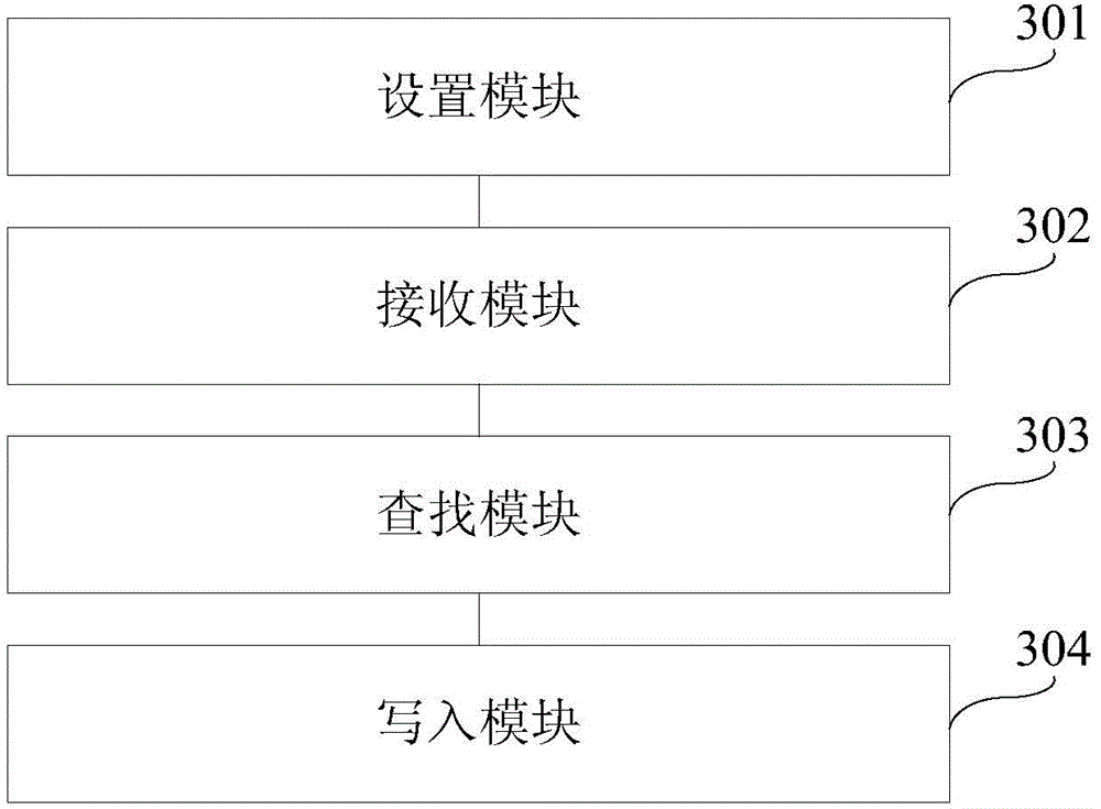
[0065] refer to image 3 , which shows a structural block diagram of an embodiment of a device for accessing chip information in the present invention, which may specifically include the following modules:

[0066] The setting module 301 is configured to pre-configure an independent storage space in the chip, and set at least two levels of storage areas in the independent storage space.

[0067] The receiving module 302 is configured to receive a write instruction for writing data into the independent storage space, and obtain a user level identifier from the write instruction.

[0068] A search module 303, configured to search the independent storage space by using the user's level identifier, and determine a storage area of ​​a corresponding level.

[0069] The write module 304 is configured to write the chip production information acquired from the write ...


PUM


Abstract

The invention discloses a chip information access method and device to solve the problem that information in a chip is covered or erased. The method comprises the steps of configuring independent storage space in the chip in advance, and arranging at least two stages of storage areas in the independent storage space; receiving a write instruction writing data into the independent storage space, and obtaining a level identification of a user from the write instruction; looking up the independent storage space by the adoption of the level identification of the user, and determining the storage area of a corresponding level; writing chip production information obtained from the write instruction into the storage area of the corresponding level. By means of the chip information access method and device, it is guaranteed that the user can only write data into the storage area of the level which the user belongs to, the production information of the chip is prevented from being covered or erased, the integrality of the chip production information is guaranteed, and the quick and accurate location can be achieved when faults of the chip occur.

Description

technical field [0001] The invention relates to the field of communication technology, in particular to a method for accessing chip information and a device for accessing chip information. Background technique [0002] In the production process of hardware devices such as chips, the production information of the chip, such as the date of manufacture, is usually recorded in the chip. But in fact, since the chip may be finally completed after multiple generations, and information may be recorded in each generation, the area in the chip that records its production information may be accessed multiple times. [0003] In the process of multiple visits to the area where the production information is recorded in the chip, the information recorded in the previous production may be overwritten or erased, resulting in incomplete information. As a result, users cannot obtain complete information records when consulting information, especially when the chip fails, they cannot quickly a...

Claims


Application Information

Patent Timeline
Patent Type & Authority Applications(China)
IPC IPC(8): G06F13/16G06F12/02G06F3/06
Inventor 舒清明胡洪卜尔龙薛子恒
Owner GIGADEVICE SEMICON (BEIJING) INC
Why Eureka
Try Eureka