

Image generating device, defect inspecting device, and defect inspecting method
An image generation device and image generation technology, which are applied in image enhancement, image analysis, measurement devices, etc., can solve problems such as undetectable defects and limited defect detection capabilities, and achieve the effect of preventing repeated detection and high detection capabilities.
- Summary
- Abstract
- Description
- Claims
- Application Information
AI Technical Summary
Problems solved by technology
Method used
Image

Examples
Embodiment Construction
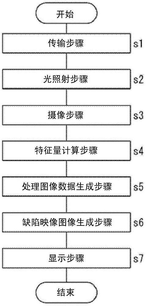
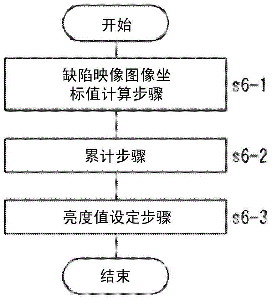
[0068] Figure 1A and 1B is a flowchart showing the steps of the defect inspection method according to one embodiment of the present invention. The defect inspection method of this embodiment includes Figure 1A The transmission step s1 , the light irradiation step s2 , the imaging step s3 , the characteristic amount calculation step s4 , the processed image data generation step s5 , the defect map image generation step s6 , and the display step s7 are shown. In addition, the defect map image generating step s6 includes Figure 1B The defect map image coordinate value calculation step s6-1, accumulation step s6-2, and brightness value setting step s6-3 are shown.
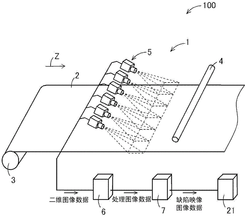
[0069] figure 2 It is a schematic diagram which shows the structure of the defect inspection apparatus 100 which concerns on one Embodiment of this invention. image 3 It is a block diagram showing the configuration of the defect inspection apparatus 100 . The defect inspection device 100 of the present embodi...
PUM
 Abstract
Description
Claims
Application Information