Fine line circuit board processing method and circuit board processing system
A technology of fine lines and processing methods, which is applied in the direction of removing conductive materials by chemical/electrolytic methods, and can solve the problems of low production efficiency of front and back etching processes, discrepancies between actual and theoretical conditions, and inoperability of front and back etching processes, etc. , to achieve the effect of reducing open circuit or short circuit and unqualified line width, solving open circuit or short circuit and unsuitable line width, and saving engineering production time
- Summary
- Abstract
- Description
- Claims
- Application Information
AI Technical Summary
Problems solved by technology
Method used
Image
Examples
Embodiment 1
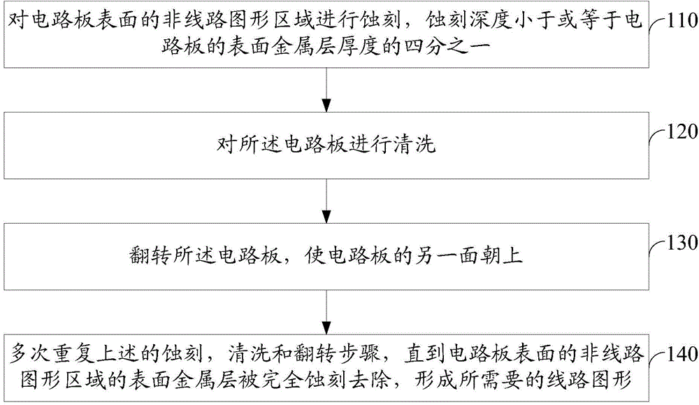
[0023] Please refer to figure 1 , an embodiment of the present invention provides a method for processing a fine circuit board, which may include:
[0024] 110. Etching the non-circuit pattern area on the surface of the circuit board, the etching depth is less than or equal to 1 / 4 of the thickness of the metal layer on the surface of the circuit board.
[0025] In the embodiment of the present invention, in order to improve the uniformity of etching, the conventional one-time etching is decomposed into multiple etchings. The multiple times of etching are at least four times, and the etching depth of each etching is at least 1 / 4 of the thickness of the metal layer on the surface of the circuit board.
[0026] Wherein, before etching, a surface treatment step may be included, for example, it may specifically include cleaning and micro-etching, etc. to remove dirt and oxides on the surface of the circuit board to facilitate subsequent treatment.
[0027] In this step, before et...
Embodiment 2
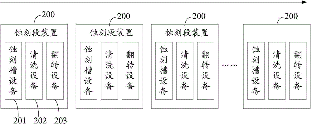
[0040] Please refer to figure 2 , the embodiment of the present invention provides a circuit board processing system, the system includes: at least four sets of etching segment devices 200; wherein each group of etching segment devices includes:
[0041] The etching tank device 201 is used to etch the non-line pattern area on the surface of the circuit board, and the etching depth is less than or equal to a quarter of the thickness of the metal layer on the surface of the circuit board;
[0042] Cleaning equipment 202, cleaning the circuit board etched through the etching tank;
[0043] Turning device 203 is used to turn over the circuit board cleaned by the cleaning device so that the other side of the circuit board faces upward.
[0044] In some embodiments of the present invention, the system also includes:
[0045] a film removing device, used to remove the resist film provided on the circuit board;
[0046] a cleaning device, used to clean the circuit board after film...
PUM
 Abstract
Description
Claims
Application Information
 - R&D Engineer
- R&D Manager
- IP Professional
- Industry Leading Data Capabilities
- Powerful AI technology
- Patent DNA Extraction
Browse by: Latest US Patents, China's latest patents, Technical Efficacy Thesaurus, Application Domain, Technology Topic, Popular Technical Reports.
© 2024 PatSnap. All rights reserved.Legal|Privacy policy|Modern Slavery Act Transparency Statement|Sitemap|About US| Contact US: help@patsnap.com


