Field cut-off current control type power device with self-adaption

A technology for current control and power devices, applied in electrical components, semiconductor devices, circuits, etc., can solve the problem of no field cut-off function, and achieve the effect of getting rid of limited diffusion depth and enhancing adaptive characteristics

Active Publication Date: 2018-05-18
中国东方电气集团有限公司
View PDF4 Cites 0 Cited by
  • Summary
  • Abstract
  • Description
  • Claims
  • Application Information

AI Technical Summary

Problems solved by technology

Although the above-mentioned comparative document introduces a trench on the back of the device, the trench is set in the P+ collector region. The trench does not have a field stop function, but only forms a new collector region structure. The N+ buffer zone set between the P+ collector region and the N-drift region is the field stop layer, and the field stop layer is still realized by the traditional doping method.

Method used


Image

  • Field cut-off current control type power device with self-adaption
  • Field cut-off current control type power device with self-adaption
  • Field cut-off current control type power device with self-adaption

Examples


Embodiment 1

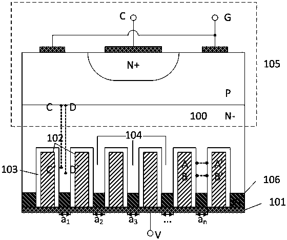
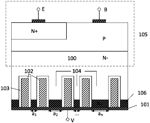
[0031] The self-adaptive field cut-off current control type power device includes a metal conductive layer 101, and one side of the metal conductive layer 101 is provided with a substrate or a substrate epitaxial layer 100, where the substrate or substrate epitaxial layer 100 is two In an alternative relationship, according to the structure of the device and the corresponding process, it can be the substrate or the epitaxial layer of the substrate. The substrate refers to the directly purchased substrate substrate, such as single crystal silicon, and the substrate epitaxial layer refers to a layer of single crystal thin film grown by epitaxy on the purchased substrate substrate. Take PNPN type GTO as an example, such as figure 1 , use an N-type substrate, form a P base region and an N emitter, that is, a cathode, by diffusion on the front side, and form a P emitter, that is, an anode, by diffusion on the back side. At this time, the label 100 is actually the substrate. Take t...

Embodiment 2

[0034] The self-adaptive field cut-off current control type power device includes a metal conductive layer 101, and one side of the metal conductive layer 101 is provided with a substrate or a substrate epitaxial layer 100, where the substrate or substrate epitaxial layer 100 is two In an alternative relationship, according to the structure of the device and the corresponding process, it can be the substrate or the epitaxial layer of the substrate. The substrate refers to the directly purchased substrate substrate, such as single crystal silicon, and the substrate epitaxial layer refers to a layer of single crystal thin film grown by epitaxy on the purchased substrate substrate. Take PNPN type GTO as an example, such as figure 1 , use an N-type substrate, form a P base region and an N emitter, that is, a cathode, by diffusion on the front side, and form a P emitter, that is, an anode, by diffusion on the back side. At this time, the label 100 is actually the substrate. Take t...

Embodiment 3

[0042] The self-adaptive field cut-off current control type power device includes a metal conductive layer 101, and one side of the metal conductive layer 101 is provided with a substrate or a substrate epitaxial layer 100, where the substrate or substrate epitaxial layer 100 is two In an alternative relationship, according to the structure of the device and the corresponding process, it can be the substrate or the epitaxial layer of the substrate. The substrate refers to the directly purchased substrate substrate, such as single crystal silicon, and the substrate epitaxial layer refers to a layer of single crystal thin film grown by epitaxy on the purchased substrate substrate. Take PNPN type GTO as an example, such as figure 1 , use an N-type substrate, form a P base region and an N emitter, that is, a cathode, by diffusion on the front side, and form a P emitter, that is, an anode, by diffusion on the back side. At this time, the label 100 is actually the substrate. Take t...


PUM


Abstract

The invention relates to the field of semiconductor devices, in particular to a field cut-off current control power device with adaptivity. The field cut-off current control power device comprises a metal conductive layer, wherein a substrate or a substrate epitaxial layer is arranged at one side of the metal conductive layer; a plurality of channels are formed in the substrate or the substrate epitaxial layer; a front-side structure of a current control power device is arranged at one side of the substrate or the substrate epitaxial layer; a potential V end is arranged on the metal conductive layer at one side of each channel; a back heavily doped region is also arranged between the metal conductive layer and the substrate or the substrate epitaxial layer; channel-type conductive fillers are arranged in various channels; insulating layers are arranged on the side wall and the bottom of each channel; and inductive charge concentration enhancement regions are formed among various channels. According to the field cut-off current control power device, a field cut-off technology is introduced into a traditional current control device, so that the problem that relatively high withstand voltage is achieved on a relatively thin chip is solved; field cut-off is achieved through a device structure design; and the defects that the inherent diffusion depth is limited, other structures of the device are affected by a high-temperature process, the process is limited and the like in the prior art are overcome.

Description

technical field [0001] The invention relates to the field of semiconductor devices, in particular to an adaptive field cut-off current control type power device. Background technique [0002] Gate Turn-Off Thyristor (Gate Turn-Off Thyristor, GTO), also known as gated thyristor, is a type of current-controlled power device, which maintains the advantages of high withstand voltage and large current of traditional thyristor. It has self-shutoff capability and is easy to use. It is an ideal high-voltage and high-current switching device and can be used to form high-power inverters, circuit breakers, phase controllers and various switching circuits. [0003] Bipolar Junction Transistor (BJT), like GTO, is also a current-controlled power device. It has the advantages of small size, light weight, low power consumption, long life, and high reliability. It is widely used in broadcasting, In the fields of television, communication, radar, computer, automatic control device, electroni...

Claims


Application Information

Patent Timeline
Patent Type & Authority Patents(China)
IPC IPC(8): H01L29/745H01L29/73H01L29/861H01L29/872H01L29/06
CPCH01L29/0684H01L29/73H01L29/745H01L29/861H01L29/872
Inventor 胡强蒋兴莉孔梓玮王思亮张世勇
Owner 中国东方电气集团有限公司
Why Eureka
Try Eureka