A Device Structure Using Trench Field Effect to Realize Adaptive Field Stop Technology

A device structure and self-adaptive technology, applied in semiconductor devices, electrical components, circuits, etc., can solve problems such as impact, process limitations, and limited diffusion depth

Active Publication Date: 2018-05-18
中国东方电气集团有限公司
View PDF4 Cites 0 Cited by
  • Summary
  • Abstract
  • Description
  • Claims
  • Application Information

AI Technical Summary

Problems solved by technology

We have mentioned above that there are two disadvantages in this traditional method, one is the limited diffusion depth, and the other is the high temperature process
For example, if phosphorus diffuses 7 microns in silicon, it needs to be diffused at a high temperature of 1150 degrees Celsius for 400 minutes, which will have a serious impact on other structures of the device and greatly limit the process.

Method used


Image

  • A Device Structure Using Trench Field Effect to Realize Adaptive Field Stop Technology
  • A Device Structure Using Trench Field Effect to Realize Adaptive Field Stop Technology
  • A Device Structure Using Trench Field Effect to Realize Adaptive Field Stop Technology

Examples


Embodiment 1

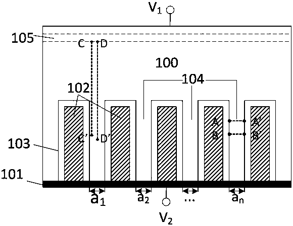
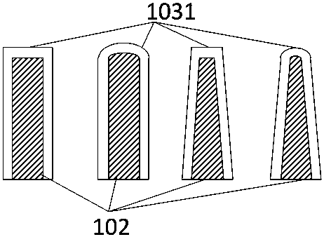
[0033] A device structure using trench field effect to realize adaptive field stop technology includes a metal conductive layer 101, a substrate 100 is arranged on one side of the metal conductive layer 101, and a plurality of grooves are arranged on the substrate 100, One side of the substrate 100 is provided with a depletion region 105, one side of the depletion region 105 is provided with a potential V1, and the metal conductive layer 101 on one side of the trench is provided with a potential V2; each trench is provided with a trench The trench conductive filling 102 is provided with an insulating layer 103 on the sidewall and bottom 1031 of the trench, and the interconnected induced charge concentration enhancement regions 104 are formed between the trenches. The widths of the induced charge concentration enhanced regions 104 are respectively a1, a2, . . . , an, wherein n represents the number of the induced charge concentration enhanced regions 104 . The interconnected in...

Embodiment 2

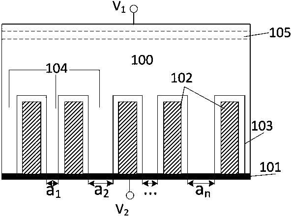
[0036] A device structure using trench field effect to realize adaptive field stop technology includes a metal conductive layer 101, a substrate 100 is arranged on one side of the metal conductive layer 101, and a plurality of grooves are arranged on the substrate 100, One side of the substrate 100 is provided with a depletion region 105, one side of the depletion region 105 is provided with a potential V1, and the metal conductive layer 101 on one side of the trench is provided with a potential V2; each trench is provided with a trench Groove conductive filling 102, an insulating layer 103 is arranged on the side walls of the trench and the bottom 1031 of the trench, and interconnected induced charge concentration enhanced regions 104 are formed between each trench, and the widths of each induced charge concentration enhanced region 104 are respectively are a1, a2, . . . , an, wherein n represents the number of induced charge concentration enhancement regions 104 .

[0037] T...

Embodiment 3

[0048] A device structure using trench field effect to realize adaptive field stop technology includes a metal conductive layer 101, a substrate 100 is arranged on one side of the metal conductive layer 101, and a plurality of grooves are arranged on the substrate 100, One side of the substrate 100 is provided with a depletion region 105, one side of the depletion region 105 is provided with a potential V1, and the metal conductive layer 101 on one side of the trench is provided with a potential V2; each trench is provided with a trench The trench conductive filler 102 is provided with an insulating layer 103 on the trench sidewall and the trench bottom 1031 , and an induced charge concentration enhancement region 104 connected to each other is formed between the trenches. The widths of the induced charge concentration enhanced regions 104 are respectively a1, a2, . . . , an, wherein n represents the number of the induced charge concentration enhanced regions 104 .

[0049] Th...


PUM


Abstract

The invention relates to the field of semiconductor devices, in particular to a device structure for achieving an adaptive field cut-off technology through the channel field effect. The device structure comprises a metal conductive layer, wherein a substrate is arranged at one side of the metal conductive layer; a plurality of channels are formed in the substrate; an exhaust region is arranged at one side of the substrate; potential V1 is set at one side of the exhaust region; potential V2 is set on the metal conductive layer at one side of each channel; channel-type conductive fillers are arranged in various channels; insulating layers are arranged on the side wall and the bottom of each channel; and interconnected inductive charge concentration enhancement regions are formed among various channels. According to the device structure, field cut-off is achieved through a device structure design; the defects that the inherent diffusion depth is limited, other structures of the device are affected by a high-temperature process, the process is limited and the like in the prior art are thoroughly overcome; the field cut-off function of the device structure is achieved through the channel field effect; and the effect has adaptive characteristics which are enhanced along with electrical field enhancement.

Description

technical field [0001] The invention relates to the field of semiconductor devices, in particular to a device structure which adopts trench field effect to realize self-adaptive field stop technology. Background technique [0002] During the development of power semiconductor devices, field stop technology was introduced in order to achieve higher withstand voltage on thinner chips. The field stop is usually implemented in the form of high-concentration doping, so that the electric field rapidly decays to zero after the boundary of the depletion region reaches the field stop layer, so as to avoid the breakdown caused by the punch-through of the depletion region. Field stop technology is commonly used in diodes, triodes, MOS tubes, and insulated gate bipolar transistors. [0003] According to Poisson's equation for electrostatic field [0004] [0005] is the electric potential, is the charge density, is the vacuum permittivity, is the relative permittivity. [...

Claims


Application Information

Patent Timeline
Patent Type & Authority Patents(China)
IPC IPC(8): H01L29/06H01L29/423H01L29/78
CPCH01L29/0638H01L29/4236H01L29/78
Inventor 胡强蒋兴莉孔梓玮王思亮张世勇
Owner 中国东方电气集团有限公司
Why Eureka
Try Eureka