

Mapping table forming and loading methods and electronic device
An electronic device and mapping table technology, applied in the electronic field, can solve the problems of huge metadata mapping table information and long response time of the hard disk when starting up, and achieve the effect of improving user experience and shortening the time.
- Summary
- Abstract
- Description
- Claims
- Application Information
AI Technical Summary
Problems solved by technology
Method used
Image

Examples
Embodiment 1
[0076] Embodiments of the present invention provide a method for forming a mapping table, which is applied to electronic equipment. The functions implemented by the method for forming the mapping table can be implemented by calling program codes from the SSD controller in the electronic equipment. Of course, the program codes can be stored in the computer. In the storage medium, it can be seen that the electronic device at least includes an SSD controller and a storage medium.
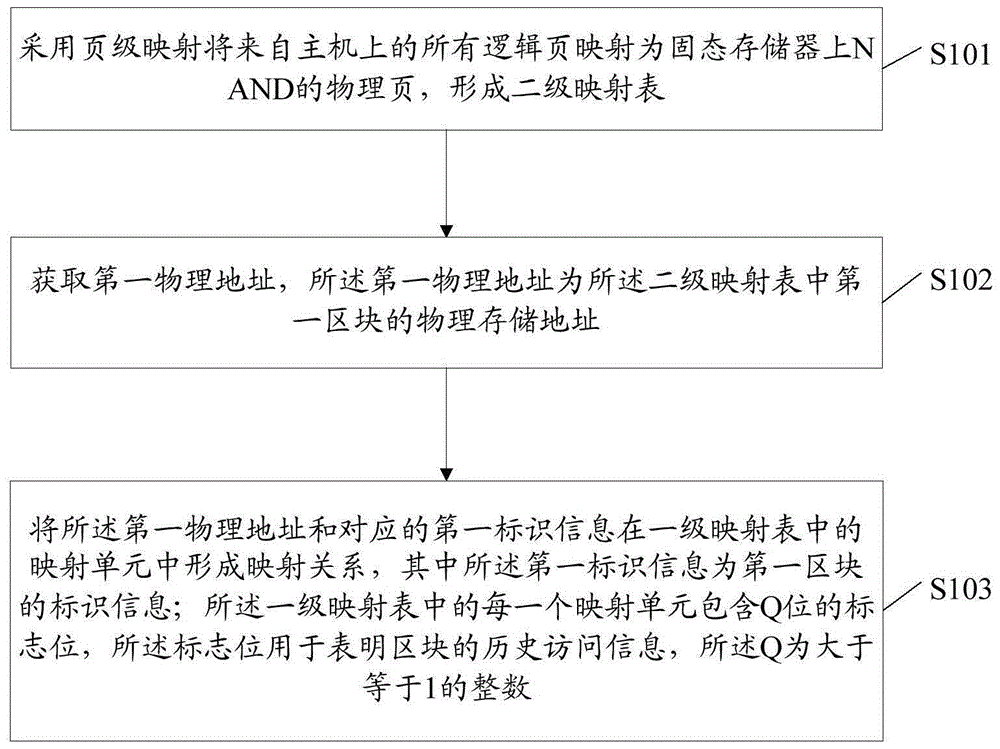
[0077] Picture 1-1 It is a schematic diagram of the implementation flow of the method for forming a mapping table in Embodiment 1 of the present invention, as Picture 1-1 As shown, the method includes:
[0078] Step S101, using page-level mapping to map all logical pages from the host to physical pages of NAND on the solid-state memory to form a secondary mapping table;
[0079] Here, the mapping table includes a primary mapping table and a secondary mapping table; the host refers to an electronic de...
Embodiment 2
[0101] Based on the aforementioned embodiments, the embodiment of the present invention provides a method for forming a mapping table, which is applied to an electronic device. The functions implemented by the method for forming a mapping table can be implemented by calling program codes from the SSD controller in the electronic device. Of course, The program code can be stored in a computer storage medium. It can be seen that the electronic device at least includes an SSD controller and a storage medium.
[0102] figure 2 It is a schematic diagram of the implementation flow of the method for forming the mapping table in Embodiment 2 of the present invention, as figure 2 As shown, the method includes:
[0103] Step S201, using page-level mapping to map all logical pages from the host to physical pages of NAND on the solid-state memory to form a secondary mapping table;
[0104] Here, the mapping table includes a primary mapping table and a secondary mapping table; the host...
Embodiment 3
[0116] Based on the foregoing embodiments, the embodiment of the present invention further provides a method for loading a mapping table, which is applied to an electronic device. The functions implemented by the method for forming the mapping table can be implemented by calling program codes from the SSD controller in the electronic device. Of course, the program code can be stored in a computer storage medium. It can be seen that the electronic device at least includes an SSD controller and a storage medium.
[0117] image 3 It is a schematic flow diagram of the implementation flow of the loading method of the mapping table in the third embodiment of the present invention, such as image 3 As shown, the method includes:
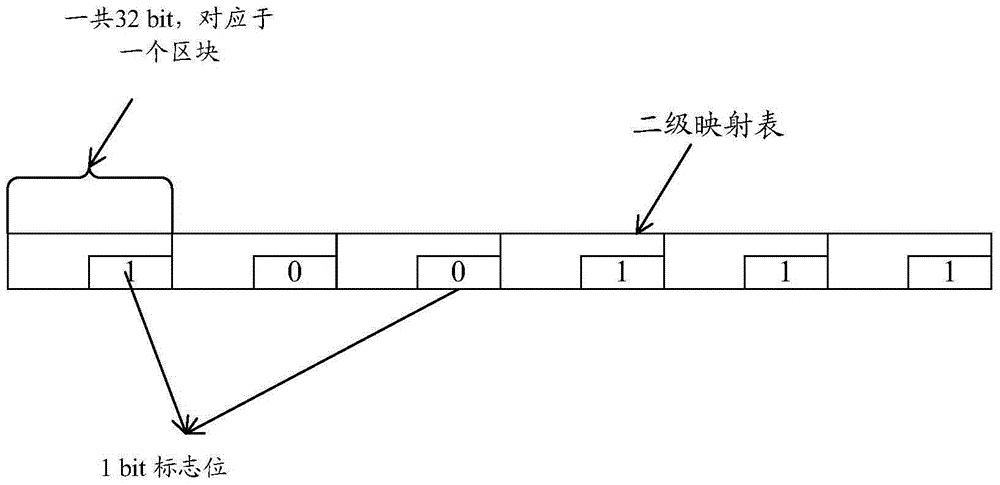
[0118] Step S301, read the flag bit on the first mapping unit in the primary mapping table, the flag bit is used to indicate whether the first block has been accessed last time, the first block is the first The block corresponding to the mapping unit;
...
PUM
 Abstract
Description
Claims
Application Information