Memory architecture with wiring structure enabling different access patterns in multiple dimensions

A technology of multiplexers and functional circuits, applied in static memory, instruments, measuring devices, etc., can solve problems such as cycle delay growth

Active Publication Date: 2017-11-17
INT BUSINESS MASCH CORP
View PDF6 Cites 0 Cited by
  • Summary
  • Abstract
  • Description
  • Claims
  • Application Information

AI Technical Summary

Problems solved by technology

Also, as the operating frequency increases, the cycle-by-cycle latency associated with communicating between processors increases

Method used


Image

  • Memory architecture with wiring structure enabling different access patterns in multiple dimensions
  • Memory architecture with wiring structure enabling different access patterns in multiple dimensions
  • Memory architecture with wiring structure enabling different access patterns in multiple dimensions

Examples


Embodiment Construction

[0058] Concerning 3-D multiprocessor devices formed by connecting multiple processors in a stacked configuration, and for controlling 3-D stacked multiprocessor devices to operate selectively in one of multiple resource pooling and sharing modes The method, the exemplary embodiment of the present invention will be described in further detail.

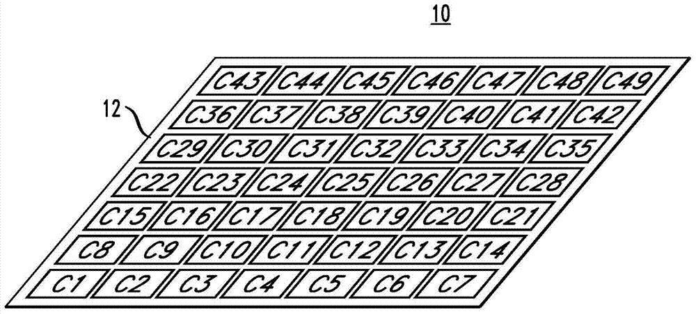
[0059] figure 1 is a schematic diagram of a multiprocessor chip to which the principles of the present invention may be applied. specifically, figure 1 A multiprocessor chip 10 is schematically depicted, comprising a semiconductor die 12 with a plurality of processors C1, C2, . . . , C49 (generally denoted Cn) on a die 12 . The processors Cn are arranged in a "planar" system, where each processor Cn has its own dedicated footprint in 2-D space. As already understood by those skilled in the art, in a 2-D plane, using horizontal wiring and electrical connections formed as part of the BEOL (back end of line) structure of the chip 10, th...


PUM


Abstract

A multidimensional memory architecture is provided that has an access wiring structure that enables different access patterns in multiple dimensions. Furthermore, a three-dimensional multiprocessor system is provided that includes a multi-dimensional cache memory architecture with an access wiring structure enabling different access patterns in multiple dimensions.

Description

[0001] cross reference [0002] This application claims priority to US Patent Application No. 13 / 927,846, filed June 26, 2013, the disclosure of which is incorporated herein by reference. technical field [0003] The technical field of the invention relates generally to multidimensional memory architectures having access wiring structures that enable different access modes in multiple dimensions, and to three-dimensional (3-D) multiprocessor systems that The system has a multi-dimensional cache memory architecture with an access wiring structure enabling different access patterns in multiple dimensions. Background technique [0004] In the field of semiconductor processor chip manufacturing, in the early stages of processor technology, many companies manufactured single-chip processors. Over the past decade or so, as Moore's Law has continued to shrink dimensions, many companies and other entities have begun designing processor chips with multiple processors on one layer. ...

Claims


Application Information

Patent Timeline
Patent Type & Authority Patents(China)
IPC IPC(8): G06F13/00
CPCG11C29/32G01R31/318536G01R31/3177
Inventor 阿尔泊·布约克托苏诺格鲁菲利普·G·埃玛艾伦·M·哈特斯坦M·B·海利K·K·凯拉斯
Owner INT BUSINESS MASCH CORP
Why Eureka
Try Eureka