Multipath switching circuit, chip and communication terminal

A switching circuit and multi-path technology, applied in electronic switches, electrical components, transmission systems, etc., can solve the problems of RF signal leakage, degree of saturation of performance improvement, affecting the linearity characteristics of switches, etc., to achieve simple circuits and methods, improve linearity characteristics, the effect of improving the switching loss

Inactive Publication Date: 2016-04-20
VANCHIP TIANJIN TECH
View PDF9 Cites 10 Cited by
  • Summary
  • Abstract
  • Description
  • Claims
  • Application Information

AI Technical Summary

Problems solved by technology

In addition, on the one hand, when each switching transistor is turned on, since there are parasitic capacitances between the source and the gate and the drain and the gate of the switching transistor, a part of the radio frequency signal will leak from the source and the drain to the gate, Thus affecting the differential loss characteristics of the switch; on the other hand, when the switching transistor is turned off, the channel between its source and drain is closed, but there is also a parasitic capacitance between the source and drain, which will also affect the switch's Linearity
[0006] In the prior art, for a given integrated circuit process, although increasing the gate width of the transistor can reduce the differential loss of the switch and improve the linearity, it is limited by the chip area, that is, the design cost; at the same time, due to the parasitic Capacitance, its degree of performance improvement will gradually become saturated
On the other hand, although many semiconductor manufacturers are currently committed to developing new processes and switching devices, their development cycle is long and the cost is high.

Method used


Image

  • Multipath switching circuit, chip and communication terminal
  • Multipath switching circuit, chip and communication terminal
  • Multipath switching circuit, chip and communication terminal

Examples


Embodiment 1

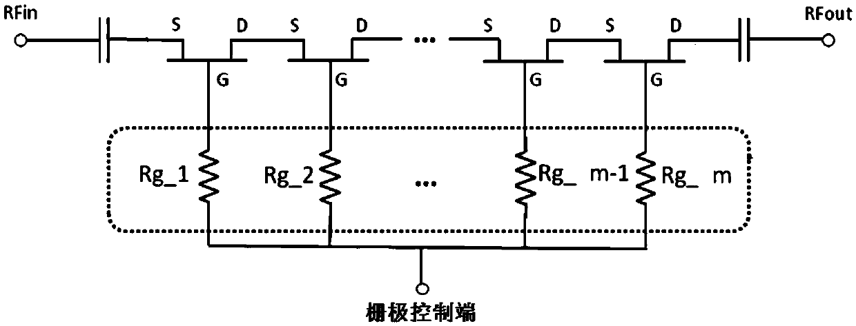
[0036] refer to image 3 As shown, it is a schematic diagram of a multipath switch circuit according to Embodiment 1 of the present invention. The multipath switch circuit includes: a series-connected common gate switch transistor group, a source-drain bias resistor network 101, and a gate bias resistor network 102, wherein :

[0037] In the common gate switching transistor group, the source of the first switching transistor is connected to the RF signal input terminal RFin of the switch path through a DC blocking capacitor, and the drain of the last switching transistor is connected to the RF signal input terminal RFin of the switching path through a DC blocking capacitor. The signal output terminals RFout are connected; and the drains and sources of other adjacent switching transistors in the common gate switching transistor group are sequentially connected in series;

[0038] The source-drain bias resistor network 101 is arranged between the source of the first switching t...

Embodiment 2

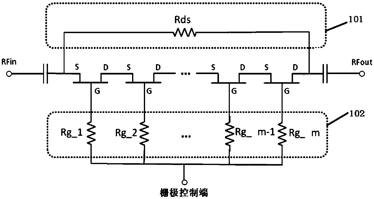
[0042]refer to Figure 4 As shown, it is a schematic diagram of the multi-path switch circuit in Embodiment 2 of the present invention. Similar to Embodiment 1, the multi-path switch circuit includes: a series-connected common-gate switch transistor group, a source-drain bias resistor network 101, a gate The bias resistor network 102, but for the source-drain bias resistor network 101, the gate bias resistor network 102 is further improved compared to the first embodiment, wherein:

[0043] The source-drain bias resistor network 101 includes: a number of resistors (Rds_1, Rds_2, ..., Rds_m) that are equal to and correspond to the number of switch transistors in the common gate switch transistor group, and each resistor is set in parallel between the source and the drain of the corresponding switching transistor and sequentially connected in series;

[0044] The gate bias resistor network 102 includes: a number of individual gate bias resistors Rg_1, Rg1, . . . One end of the...

Embodiment 3

[0047] refer to Figure 5 As shown, it is a schematic diagram of the multi-path switch circuit in Embodiment 3 of the present invention. Similar to Embodiment 2, the multi-path switch circuit includes: a series-connected common-gate switch transistor group, a source-drain bias resistor network 101, a gate The bias resistor network 102, but the gate bias resistor network 102 is further improved compared to the second embodiment, wherein:

[0048] The gate bias resistor network 102 includes: a number of individual gate bias resistors Rg_1, ..., Rg_m, Rg_m that are equal to the number of switch transistors (2m) in the common gate switch transistor group and correspond one-to-one +1, ..., Rg_2m, and the first common gate bias resistor Rgc_1, the second common gate bias resistor Rgc_2; one end of each individual gate bias resistor is respectively connected to the gate of the corresponding switching transistor , and several of the individual gate bias resistors are divided into two...


PUM


Abstract

The invention discloses a multipath switching circuit applied in a solid antenna switch. The multipath switching circuit comprises common gate switch transistor groups connected in series and arranged between a radio-frequency signal input end and a signal output end, and a source drain bias resistor network arranged between a source of a first crystal switch tube which is connected to the signal input end and a drain of a last crystal switch tube which is connected to the signal output end. The multipath switch circuit provided by the invention can effectively improve linear characteristics of a path switch. The invention further discloses a chip including the multipath switch circuit and a communication terminal including the multipath switch circuit or the chip.

Description

technical field [0001] The invention relates to a multi-path switch circuit for a solid-state antenna switch, a chip containing the circuit and a communication terminal, belonging to the technical field of integrated circuits. Background technique [0002] Solid-state antenna switches have been widely used in wireless mobile communication front-end modules or multi-path antenna switch modules. In the rapidly developing multi-mode and multi-band smartphone system, the number of modes and frequency bands is constantly increasing, which requires more and more paths in the antenna switch, while maintaining or even improving its dropout and linearity characteristics . [0003] In the prior art, the structural block diagram of a typical multipath antenna switch is as follows figure 1 shown. When the switch of one of the paths is turned on, the switches of other paths are turned off at the same time, so that only the radio frequency signal connected to this path can be transmitt...

Claims


Application Information

Patent Timeline
Patent Type & Authority Applications(China)
IPC IPC(8): H03K17/94
CPCH03K17/94H03K17/693H03K2217/0054H04B1/006H04B1/1081
Inventor 林升
Owner VANCHIP TIANJIN TECH
Why Eureka
Try Eureka